Paul I apologise, had to make a urgent business trip but I will have a look at your simulation file during the weekend. Can you supply your model file as well so we have the same .
I tried your compensation scheme on my amp but in my case I not only had a little peaking I couldnt get rid of but distortion was also a little worse off. The only diffrence in topology is that I have no error corection scheme, maybe this has some influence. Im very wary of any peaking in the closed loop response especially with current feedback, at times Ive found as little as .5db could cause a amp to start oscilating with certain speaker cables, long runs of cables and some speaker loads.
Excellent results in post 31. Impressive.
Manso, no need to apologise we all have busy lives
Most of the transistor models are from Bob cordell's site. There is a text page you can use. Attached is the exicon zip file of models I'm using the ECF20N20 and and ECF20P20.
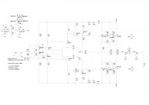
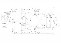
I have a new version of my amp it has a cascode VAS now ( i know I wasn't going to use cascodes but....) It has a compensation scheme more normal to CFB amps. It has not been fine tuned though. Here is the .asc file so you know where I'm at.
The circuit in post 31 had questionable stability.
Paul
Most of the transistor models are from Bob cordell's site. There is a text page you can use. Attached is the exicon zip file of models I'm using the ECF20N20 and and ECF20P20.
I have a new version of my amp it has a cascode VAS now ( i know I wasn't going to use cascodes but....) It has a compensation scheme more normal to CFB amps. It has not been fine tuned though. Here is the .asc file so you know where I'm at.
The circuit in post 31 had questionable stability.
Paul
Attachments
Last edited:
Apex (DC Offset) vs Hifisonix (AFEC) vs mcd99uk
Went back to basics. Took some ideas off Apex and his FX8SCF. By chance the first version of this amp resembled his amplifier. Then having read a paper on distortion only feedback and having previously experimented with Hifisonix AFEC I decided to go back to a more basic amp that was stable producing half decent THD figures and then add on a small dose of AFEC.
Also, reduced the number of cascaded transistors. The amp was much easier to compensate than the others.
The result is this creation.... No HEC only distortion feedback. It doesn't care about low impedance loads and doesn't seem to mind reactive loads.
Figures... All into 8R.
THD @ 20k +/- 2V = 0.000027%
THD @ 20k +/- 32V = 0.001224%
THD @ 1k +/- 2V = 0.000133%
THD @ 1k +/- 32V = 0.000644%
Not outstanding figures but low enough for pcb layout to be the limiting factor. Could wind the AFEC up a bit but this can wait until potential real world experimentation. Still got some tweaking to do anyway, like adding baker clamps etc.
The only down side is a small overshoot on square waves.
What do people think of this one?
Paul
Attachments
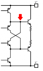
- Gain at DC is 21X so you'll need a means to trim the output offset, or nullify it with a servo. Do the opamps @ leftside also perform this function?
- Maybe there's a way to connect the collectors of Q9 and Q10 so their VCE is constant even when passing large amplitude waveforms. If so this would reduce distortion.
- R28+C12 appear to frequency compensate Q7. Why not connect them from base to collector, rather than from base to not-the-collector?
- What's the power dissipated in R39 when driving a just-barely-clipped 20 kHz sinewave into an 8 ohm load?
- I would hope that the DC bias current in the drivers Q7, Q8 is at least 100 mA, for good control of the MOSFET output stage when slewing. But low-VTH MOS transistors and R26= 120 ohms suggest that driver stage bias is much lower. What's the simulated value of Ic(Q7)?
Thank you for reviewing my circuit.
Resistors R24 and R25 represent a 10k variable resistor and the opamp circuit reflects the dc component over to the output of the amplifier. I have considred a dc servo between the input of the amp and the output. Can't do a normal servo which connects to the summing node as it fights with AEFC. Going for a DC servo does give lower distortion and come to think of it may use less components.
Should be possible. Some sort of cascode like arrangement. Have to have a think about how it could be done.
R28 and C12 was included to load the VAS at high frequencies and add some amplifier compensation. Without these networks the ability to drive capacitive loads is very much reduced.
The power dissipated when clipping is 5W.
In the current setup, you're right, the driver stage bias is only 10mA.
Tried changing drivers to MJE150xx types and increasing the bias to 70mA. The THD increased significantly. Maybe this is caused by increased loading on the VAS. Wouldn't the output device stopper resistors limit any advantage of a much smaller R26?
Gain at DC is 21X so you'll need a means to trim the output offset, or nullify it with a servo. Do the opamps @ leftside also perform this function?
Resistors R24 and R25 represent a 10k variable resistor and the opamp circuit reflects the dc component over to the output of the amplifier. I have considred a dc servo between the input of the amp and the output. Can't do a normal servo which connects to the summing node as it fights with AEFC. Going for a DC servo does give lower distortion and come to think of it may use less components.
Maybe there's a way to connect the collectors of Q9 and Q10 so their VCE is constant even when passing large amplitude waveforms. If so this would reduce distortion.
Should be possible. Some sort of cascode like arrangement. Have to have a think about how it could be done.
[*] R28+C12 appear to frequency compensate Q7. Why not connect them from base to collector, rather than from base to not-the-collector?
R28 and C12 was included to load the VAS at high frequencies and add some amplifier compensation. Without these networks the ability to drive capacitive loads is very much reduced.
[*] What's the power dissipated in R39 when driving a just-barely-clipped 20 kHz sinewave into an 8 ohm load?
The power dissipated when clipping is 5W.
I would hope that the DC bias current in the drivers Q7, Q8 is at least 100 mA, for good control of the MOSFET output stage when slewing. But low-VTH MOS transistors and R26= 120 ohms suggest that driver stage bias is much lower. What's the simulated value of Ic(Q7)?
In the current setup, you're right, the driver stage bias is only 10mA.
Tried changing drivers to MJE150xx types and increasing the bias to 70mA. The THD increased significantly. Maybe this is caused by increased loading on the VAS. Wouldn't the output device stopper resistors limit any advantage of a much smaller R26?
Maybe the alleged increase in predicted distortion is more to do with swapping the transistor models.
Yes, I tend to agree because given that hfe is still significant and the current is small, the loading on the VAS should still be minimal.
In reality, I plan to use bigger drivers probably either the 2SA1225/ 2SC2983. But the power dissipation of running 100mA bias is quite large and may force either a compromise or using the dreaded MJE150xx transistors. I would rather the compromise and use the lower cob transistors.
PS I like the use of the word "alleged"
The evolution continues
Here's the latest version. A lot has changed, have used the common mode loop control and associated compensation from the MCP amplifier on the Data Odyssey site. What a difference... Also, using X buffer output stage. Boosted the driver bias up to just over 100mA as well as boosting the VAS current.
Still got fine tuning to do but looking promising. Need to tune the compensation properly for best THD vs GM/PM. Also, need to decide whether to use the current sources at the front end. Might also go back to a normal output stage. Had enough of simulating for today.
It has gained a stage and become a cascade of 4 instead of 3 but losing that stage destroys the performance and strangely the amp is less stable.
THD figures... Simulation of course.
THD @ 20k +/- 2V = 0.000002%
THD @ 20k +/- 32V = 0.000151%
THD @ 1k +/- 2V = 0.000000%
THD @ 1k +/- 32V = 0.000000%
Even without the AEFC THD is respectable...
THD @ 20k +/- 32V = 0.000597%
Won't see this kind of performance in reality sadly
Attachments
Last edited:
- I'd suggest you monitor the power dissipation of predrivers Q11 and Q12 when delivering a full-amplitude, slightly clipped 20kHz sinewave into 8 ohms. Both RMS average power, and instantaneous power-vs-time. You might want a beefier package than TO-92 in those positions.
- I like your choice of drivers (Q7, 8, 21, 22) and bias current; these ought to authoritatively control the gates of the output MOSFETs, even under severe conditions.
- You might find that you prefer the low capacitance NXP diode PBMD914 (datasheet) rather than the MMSD4148. Its Cmax is 1.5 pF, while the 4148's Cmax is 4 pF.
Mark,
I shall do as you say and simulate the power dissipation of the pre drivers. May substitute in 2sa1381 and 2sc3503. then I could up the current sources supplying them. I like the idea of high biasing with MOSFET outputs. It seems to help stability into reactive loads and help THD.
I like these drivers too as they are very low cob. The SOA is a bit suspect that's why I paralleled two pairs for safety. The MJE150xx drivers are horrible in a fast amp. It made mine oscillate in ltspice even with no input signal. Then looked at the closed loop response and there was a nice peak...
Indeed, I do prefer that diode, it is a superior device.
Do you think that a ULGF of 4Mhz is asking for trouble?
I very much appreciate your help, thank you!
Paul
- I'd suggest you monitor the power dissipation of predrivers Q11 and Q12 when delivering a full-amplitude, slightly clipped 20kHz sinewave into 8 ohms. Both RMS average power, and instantaneous power-vs-time. You might want a beefier package than TO-92 in those positions.
- I like your choice of drivers (Q7, 8, 21, 22) and bias current; these ought to authoritatively control the gates of the output MOSFETs, even under severe conditions.
- You might find that you prefer the low capacitance NXP diode PBMD914 (datasheet) rather than the MMSD4148. Its Cmax is 1.5 pF, while the 4148's Cmax is 4 pF.
There really is no need for such high bias current or such high power transistors for the application, those are lateral mosfets. As there is two in parralel is there is even less of such requirement. If I remember correctly the application notes for those devices supply all the necessary and correct information.
Do you think that a ULGF of 4Mhz is asking for trouble?
No.
I'm away from my bookshelf for the next several days so I'm not able to quote chapter and verse, but I recall that 90% of the amplifiers in Bob Cordell's book have a unity loop gain frequency of 10 MHz. Look at the Bode plots; closed loop gain -3dB corner frequency is 0.5 MHz and ULGF is 10 MHz. Since closed loop gain is 20X, these numbers are in agreement. As I recall, Self's book approves of 10 MHz ULGF too, but this is well disguised; it's embedded in a discussion of "number of dBs negative feedback at 20 kHz" or some other contortion.
Since you are using extremely fast output stage devices (FETs), the amount of "excess phase" they will contribute at 10 MHz is quite small. (and at 4 MHz, even less). I expect your feedback loop will be very stable when compensated for 4 MHz ULGF. Using the considerably slower bipolar pair MJL3281A/1302A, whose fTs are "only" 40 MHz, I get stable and solid performance at 10 MHz ULGF.
(It may give you a giggle to extract the "equivalent fT" of your MOSFET's spice model: Run an AC analysis with the device biased at VDS=10 and IDS=1 amp. Apply an AC current source to the gate and plot (Idrain/Igate) versus frequency. Where this curve crosses below 0dB is the "equivalent fT", i.e., the frequency at which the device ceases amplifying. I betcha it's waaaaay above 40 MHz. Meaning: it's a durn fast sumbitch, pardner.)
Done the peak and RMS values of dissipation in the pre drivers, I think I have got this right. Peak was about 1.3W and RMS was about 845mW. Way too much for a T092 device especially, if I go SMD. Substituted in the 2sa1381/2sc3503 adjusted bias and back to where I was for THD.
Have been looking at the Semelab aplication note for the ALF MOSFETS and they seem to recommend a bias of between 5 and 10mA. Not sure what to do at present. I see value and understand the benefits of both approaches.
Been messing with the compensation a little have 73 degrees PM and 13 dB GM and 20K THD of 0.000136%.
Decided that i will at least allow for boosted rails. It costs nothing extra as I have the necessary components and was planning dual supply anyway.
Is it worth implementing a basic current limiting circuit? I have read that Laterals are less prone to destroying themselves due to short circuit. My gut feel is that they will need a basic circuit.
Now for the diode change.
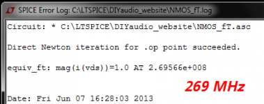
Edit: Extracted the Ft from the models and it was somewhere around 400Mhz
Have been looking at the Semelab aplication note for the ALF MOSFETS and they seem to recommend a bias of between 5 and 10mA. Not sure what to do at present. I see value and understand the benefits of both approaches.
Been messing with the compensation a little have 73 degrees PM and 13 dB GM and 20K THD of 0.000136%.
Decided that i will at least allow for boosted rails. It costs nothing extra as I have the necessary components and was planning dual supply anyway.
Is it worth implementing a basic current limiting circuit? I have read that Laterals are less prone to destroying themselves due to short circuit. My gut feel is that they will need a basic circuit.
Now for the diode change.
Edit: Extracted the Ft from the models and it was somewhere around 400Mhz
Extracted the Ft from the models and it was somewhere around 400Mhz
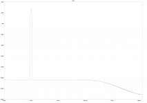
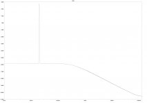
Yup. The Cordell Audio website's model of the IRFP240 (vertical channel HEXFET switching transistor) yields fT > 250 MHz, image attached.
Attachments
It's almost 1am. Time to call it a night.
The diode change resulted in no change in THD. Used the nxp model. I'm happier with this result as it is a superior device and probably a better model than the LTspice built in MMSD4148. Also, got the 20Khz (+/- 32V) THD down to 0.000124% with a change to the AFEC compensation capacitor. I think the changes to the compensation earlier allowed this to be done without affecting ability to drive reactive loads.
Have been looking at the section on current limiting in Bob Cordell's book and am currently leaning towards the opto/triac solution. I like the fact that its either on or off. It's also very simple. This circuit doesn't seem to accept natural current limiting as it just oscillates.
Yep. MOSFETs are very fast.
It might be interesting to see what happens if you also model some of the parasitics of the passive components, and then also the conductors. For example, right click on each cap and add ESR and ESL estimates for whatever frequency you are simulating (and maybe set the other parasitics explicitly to zero so they don't use default values). Later, you could estimate the length of each conductor and add an inductor in each one, with about 25 nH per inch (and 1 milliohm per inch as its ESR).
By the way, there are frequency-dependent electrolytic cap models available through Cornel Dubilier's website, from their Java Applet, which work well in transient simulations (unlike s-domain models of same, using controlled sources). Their use was explained further in the thread about paralleling electrolytic and film caps.
By the way, there are frequency-dependent electrolytic cap models available through Cornel Dubilier's website, from their Java Applet, which work well in transient simulations (unlike s-domain models of same, using controlled sources). Their use was explained further in the thread about paralleling electrolytic and film caps.
gootee, this is my next challenge. been playing with that Java Applet, good for large value capacitances by the looks of it. 10uF electrolytics are an issue at present. I plan to use panasonic FC / FM in the prototype build. The datasheets are less than helpful. I will be using C0G cermics for filter / compensation caps and have estimated the ESR at 0.1R. Not sure how to estimate the ESL though.
Have put some figures into the ESR and ESL fields for the electrolytics on the power rails and done an FFT on them 20KHz and above 1Mhz it goes very messy. Time to do a detailed read on that thread you mentioned. Only skimmed it at present.
Good thing about the PCB layout software I use is that it has calculators for track inductance and resistance. It can measure track length and then you fire the figures into the calculators along with copper weight and the numbers are there ready to paste into LTspice.
Thank you for the help.
Paul
- Status
- This old topic is closed. If you want to reopen this topic, contact a moderator using the "Report Post" button.
- Home
- Amplifiers
- Solid State
- Amp design attempt number 2 (simpler)