Ok, I've decided to go for my next ACA build. I going to try some new (to me) methods and materials in the chassis build, and I'll chronicle that in a build thread. But I'll be posting here to ask some technical questions.
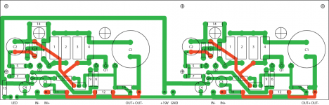
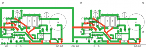
I've decided a DIY PCB is the way to go on this build, something I've never done before. I tried Eagle, but the learning curve was too steep for my now officially middle-aged brain. So I cobbled together a layout in Illustrator... see the attached image. I know nothing about PCB layout, as you may have figured out, so I'd like any input you may be able to offer. How many cardinal rules of PCB layout did I break?
Since I'll be using IRFP150s instead of 240s, what other changes need to be made, other than halving the values of the power resistors? How many amperes does the circuit draw when using the IRFP150s?
A few notes:
• To facilitate removal of the PCB/heatsink subassembly, I'll be using Molex terminal blocks or other connectors for the input, output, power, fan, and LED connections.
•I've yet to decide on a fan control circuit, so it is not yet included in the PCB layout.
• All lead spacings are approximate, and will be confirmed later.
•The four largish holes in the PCB are there to allow removal of the MOSFET mounting screws, so the boards can be removed along with the MOSFETs without having to desolder them.
Any feedback would be greatly appreciated!
Attachments
Ok, I've decided to go for my next ACA build. I going to try some new (to me) methods and materials in the chassis build, and I'll chronicle that in a build thread. But I'll be posting here to ask some technical questions.
I've decided a DIY PCB is the way to go on this build, something I've never done before. I tried Eagle, but the learning curve was too steep for my now officially middle-aged brain. So I cobbled together a layout in Illustrator... see the attached image. I know nothing about PCB layout, as you may have figured out, so I'd like any input you may be able to offer. How many cardinal rules of PCB layout did I break?
Since I'll be using IRFP150s instead of 240s, what other changes need to be made, other than halving the values of the power resistors? How many amperes does the circuit draw when using the IRFP150s?
A few notes:
• To facilitate removal of the PCB/heatsink subassembly, I'll be using Molex terminal blocks or other connectors for the input, output, power, fan, and LED connections.
•I've yet to decide on a fan control circuit, so it is not yet included in the PCB layout.
• All lead spacings are approximate, and will be confirmed later.
•The four largish holes in the PCB are there to allow removal of the MOSFET mounting screws, so the boards can be removed along with the MOSFETs without having to desolder them.
Any feedback would be greatly appreciated
ChuckORWC
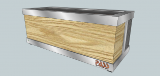
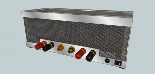
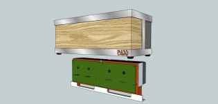
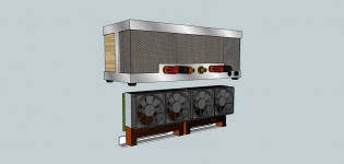
I really like your proposed case styling. Especially the second one with perforated metal sides. Perf metal is one of my favorite materials.
Nice work!
Thanks Mike,
The second image is just a rear view of the same amp. Wood up front, perf. metal rear & top. See the attached pix for views of the chassis lifted off the PCB/heatsink/fan assembly. This thing is going to be pretty small: 8 1/2"w X 3 1/4"h X 3 1/2"d. Going to be employing welding, etching, and plating, among other fun stuff. It ain't fun if it ain't challenging!
But I'd really like some input on the PCB layout...
Attachments
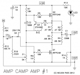
Well 2pD, there's a long way between design and successful execution... and the circuit design stuff is way over my head so I'll never equal Mr. Daniel's work.
BTW, I caught a couple of errors on the PCB layout (such as a missing trace to Q2 drain), and I added some vias where needed... New layout attached.
BTW, I caught a couple of errors on the PCB layout (such as a missing trace to Q2 drain), and I added some vias where needed... New layout attached.
Attachments
I guess I was unclear.
I want to understand how the circuit operates. Why does a change in P1 alter the voltage on the Q1 drain?
blubugeye,
P1 is a feedback loop. Here's how it works, initially Q1 is turned off. The constant current source Q2 rains down current from its source pin. Since Q1 is turned off the current has nowhere to go so the voltage before the output cap starts to rise. Now some ratio of that voltage goes to the gate of the jfet via R10, which in turn causes the voltage to rise on the gate of Q1 which pulls the current Q2 is injecting into the output to ground instead. Q1 has a threshold voltage where it starts to conduct when the gate goes a few volts higher than its source. So p1 is trimming that value to be exactly half the rail voltage. If the voltage before the cap on the output goes too high then Q1 gets turned on harder to pull down the voltage or if the voltage goes too low Q1 gets turned off a little to lift up the voltage. You see no current on your multi-meter because the jfet senses the voltage field. It’s not a current amplifier like a bipolar transistor so the current is microscopic to charge the gate of the jfet. The jfet is a follower in this mode. Which means the source voltage is just following the gate voltage, with maybe a little offset.
Hope that helps.
Last edited:
blubugeye,
... If the voltage before the cap on the output goes too high then Q1 gets turned on harder to pull down the voltage or if the voltage goes too low Q1 gets turned off a little to lift up the voltage. ...
Hope that helps.
Yes, that does help.
So, in spirit, the "resistance" presented by Q1 is adjusted by feedback through P1 and dictates the voltage at the Q1 drain.
Thanks!
So, I downloaded LTSpice, gave myself a quick crash course, and created two models: the standard ACA and the "ACA on Steroids" as suggested by Zen Mod. I used a PSU voltage of 32V and halved the values of R1-R4 as he suggested. Initial simulations show that the ACAoS indeed outputs considerably more power (how could it not?), but I'm afraid my limited comprehension of both LTSpice and amplifier design in general limits the amount of useful information I can gain from these simulations. For instance, is the power output of the circuit based upon a fixed input voltage, or is it based on the maximum input voltage that can be handled without clipping? Is output power expressed in terms of peak power, or RMS? Is there a straightforward way to measure THD in LTSpice? I know I'm exposing my ignorance here, but any guidance would be greatly appreciated.
Also, am I correct to presume that it would be a bad idea, noise-wise, to run the cooling fans off the amp's main power supply rails?
Also, am I correct to presume that it would be a bad idea, noise-wise, to run the cooling fans off the amp's main power supply rails?
Q1 drain at 0.15V regardless of pot1 position ...
Hi all.
I need some help .... Q1 stay cold
Resistors value : checked
Caps polarity : checked
Q3/Q4 pin out : checked
All solders look fine.
There's something wrong but with my low skill (close to none), I can't see it ...
Here are the voltages measured from the groundstar (with nothing to IN / OUT -) :
Should I set the PSU to 19v to check if the problem come from a to high voltage ?
?
Which component seems guilty ? How to inspect it
  ?
?
Thanks in advance and sorry to be such a newbie xD.
Hi all.
I need some help .... Q1 stay cold
Resistors value : checked
Caps polarity : checked
Q3/Q4 pin out : checked
All solders look fine.
There's something wrong but with my low skill (close to none), I can't see it ...
Here are the voltages measured from the groundstar (with nothing to IN / OUT -) :
An externally hosted image should be here but it was not working when we last tested it.
An externally hosted image should be here but it was not working when we last tested it.
Should I set the PSU to 19v to check if the problem come from a to high voltage
? Which component seems guilty
? How to inspect it ? Thanks in advance
and sorry to be such a newbie xD.R5/R6 checked : there're ok
then replace Q2 and values changed but Q1 is still cold and drain is 0.15v regardless of P1 ...
then replace Q2 and values changed but Q1 is still cold and drain is 0.15v regardless of P1 ...
An externally hosted image should be here but it was not working when we last tested it.
Here are some pics ... I may change the chassis to a bigger one later ; not a lot of space left
http://www.hostingpics.net/viewer.php?id=530767IMG20151130180349.jpg
http://www.hostingpics.net/viewer.php?id=334606IMG20151130181221.jpg
http://www.hostingpics.net/viewer.php?id=277141IMG20151130181754.jpg
PCB (from Rudi Atlos V3)
http://www.hostingpics.net/viewer.php?id=275172IMG20151130181512.jpg
If you need pics focus on something spécial : don't hesitate to ask me. My build is not really clear and I don't want to waste your time on helping me so if you need anything in order to save time : just ask.
http://www.hostingpics.net/viewer.php?id=530767IMG20151130180349.jpg
An externally hosted image should be here but it was not working when we last tested it.
http://www.hostingpics.net/viewer.php?id=334606IMG20151130181221.jpg
An externally hosted image should be here but it was not working when we last tested it.
http://www.hostingpics.net/viewer.php?id=277141IMG20151130181754.jpg
An externally hosted image should be here but it was not working when we last tested it.
PCB (from Rudi Atlos V3)
An externally hosted image should be here but it was not working when we last tested it.
http://www.hostingpics.net/viewer.php?id=275172IMG20151130181512.jpg
An externally hosted image should be here but it was not working when we last tested it.
If you need pics focus on something spécial : don't hesitate to ask me. My build is not really clear and I don't want to waste your time on helping me so if you need anything in order to save time : just ask
.I used nylon screws because they are 2.5mm diametre ... with 3mm metal the nut is too big and can't go between two heatsink's fins  .
.
Should I remove them and use metalscrew to fix the mosfet more tightly ?
What did you mean by "did you connected everything by schematic" ? I don't feel confident enought to start a project without a support to follow. On the PCB all components are set as this :
Checking before soldering, after soldering, everythings before first power up (fuse don't blow) but not working .... so start to check the PCB itself : the green et red modification on this is the only difference with initial schematic I found.
Rudi_Ratlos recently made a new layout (which works perfectly for him) with no implementation difference.
The PSU is made on veroboard using mravlca regulator schematic (http://www.diyaudio.com/forums/grou...egulator-pcb-lm317-lt1085-lm338-lt1083-8.html).
I'll inspect again tomorrow. Need resting : i'm becomming crazy to be not able to find.
. Should I remove them and use metalscrew to fix the mosfet more tightly ?
What did you mean by "did you connected everything by schematic" ? I don't feel confident enought to start a project without a support to follow
. On the PCB all components are set as this : An externally hosted image should be here but it was not working when we last tested it.
Checking before soldering, after soldering, everythings before first power up (fuse don't blow
) but not working .... so start to check the PCB itself : the green et red modification on this is the only difference with initial schematic I found.Rudi_Ratlos recently made a new layout (which works perfectly for him) with no implementation difference.
The PSU is made on veroboard using mravlca regulator schematic (http://www.diyaudio.com/forums/grou...egulator-pcb-lm317-lt1085-lm338-lt1083-8.html).
I'll inspect again tomorrow. Need resting : i'm becomming crazy to be not able to find
.ACA Concept II thread posted
Build thread for my second ACA concept (mentioned earlier in this thread) is here: ACA Concept II
-ChuckO
Build thread for my second ACA concept (mentioned earlier in this thread) is here: ACA Concept II
-ChuckO
Hi all.
I need some help .... Q1 stay cold
Resistors value : checked
Caps polarity : checked
Q3/Q4 pin out : checked
All solders look fine.
There's something wrong but with my low skill (close to none), I can't see it ...
Here are the voltages measured from the groundstar (with nothing to IN / OUT -) :
An externally hosted image should be here but it was not working when we last tested it.
An externally hosted image should be here but it was not working when we last tested it.
Should I set the PSU to 19v to check if the problem come from a to high voltage
Which component seems guilty
Thanks in advance
ChuckO
Hello again...
Ive been studying your voltage picture and I notice that there is a big difference between the Jfet Gate and Source voltages. Because this part is being used as a follower, there should not be a big difference between these voltages. And as the Pot is adjusted, the Source voltage should move in a similar fashion "following " the Gate. Also the voltage on the lower mosfets Gate is unusually high (over 6 volts) . I think this is incorrect. Maybe the Jfet is the culprit? This high voltage either is cOming from the Jfet or the lower MOSFET I think.
Last edited:
- Home
- Amplifiers
- Pass Labs
- Amp Camp Amp - ACA