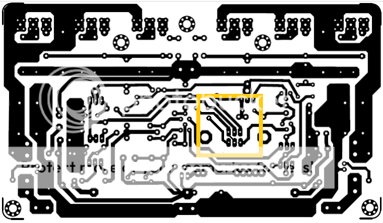
Hi Alex. I hope not to disturb you but i found a small mistake in your beautifull layout: the right side of D3 goes via R0 to E of Q20 but has to go to the base of Q7, this is not connected now.
Regards, Loek
Nice find , thank for the patience in examining the routing.
I guess that since Alex dont want to layout anymore , people
that are interested in using this PCB will have to correct themselves
the said track....

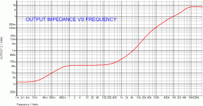
On another note , i d like to point a caracteristic of high NFB amps ,
that is , their output impedance that can be extremely low at low
frequencies and particularly at DC , no more than a few micro ohms
for the latter.
As such , an amplifier with about 2 micro ohm theorical output impedance at DC , as this one , will yield a high amplitude short circuit current if ever there is a significant output DC offset.
Assuming 10 mV DC offset and a short circuit made with a 2.5mm2 gauge wire
with 2 metres long path ( about 13 milliohm resistance), this will yield 0.77A DC output current , hence , even if an amp is not supposed to be output shorted to ground , care must be taken during build as even with no signal there s a risk if the output is shorted for a long time with eventualy higher DC offset .(a situation prevented in this amp thanks to a trimmer that is to be set such that the said offset is 1mV or less ).
Hello
I only could do anything with the Alex layout if I or someone has ability to remove from Adobe.
One of the reason I must use my own PC board layout.
The situation is interesting, until Alex helped on us many people had opinion, thoughts (not necessarily bad think) but now many of those people just disappeared.
I thought someone who has access will take care about (some one will finish) that nice job Alex gave up.
I mean at least debug the layout or take further care about if necessary..
It would be a waste to leave such a nice and well designed layout like that...
Maybe some of us are overly sceptical about the amplifier performance, I don't know.
One think is sure, I'll produce the PC boards tomorrow or Friday, I go own and build it.
Thank you wahab one more time
Greetings Gabor
Hi Alex. I hope not to disturb you but i found a small mistake in your beautifull layout: the right side of D3 goes via R0 to E of Q20 but has to go to the base of Q7, this is not connected now.
Regards, Loek
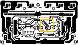
Something like this?
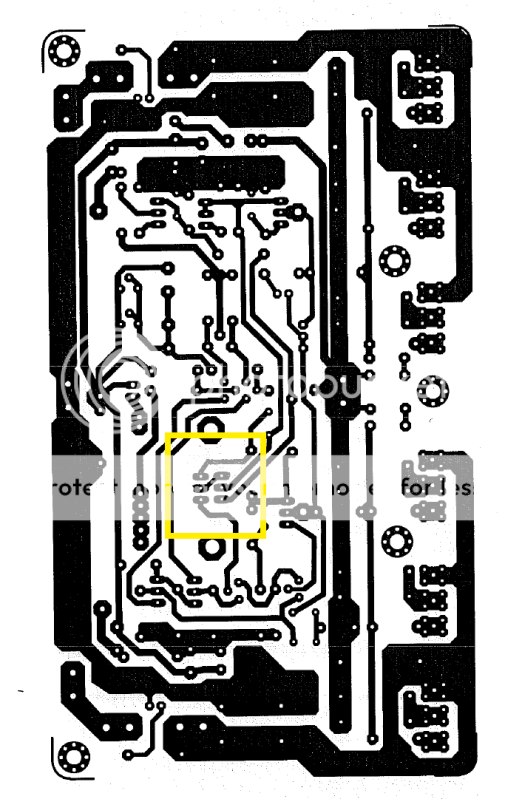
Something like this?
Check connections of C12 please
something like this?Something like this?
I see nothing.
Hello
I only could do anything with the Alex layout if I or someone has ability to remove from Adobe.
One of the reason I must use my own PC board layout.
The situation is interesting, . . .
Hello Gabor,
Have You ever check the E - mail I send to You many moons ago when You Start this nice new Fet - Amp thread ?
It is still there .... I Hope
Cheers
Hello
No is not there. I check every day my E-mail, how I did today to... Greetings Gabor
Resented again ..
Cheers
Project will be said in previous posts can be downloaded from here:
http://www.diyaudio.com/forums/soli...fi-audio-amplifier-can-run-stable-2-ohms.html
http://www.diyaudio.com/forums/soli...fi-audio-amplifier-can-run-stable-2-ohms.html
A few more simulations , particularly interesting for whom is concerned
by TIM/DIM/SID/TID , that is , that s all the names given to some
kind of Loch Ness monster that is periodicaly agitating the audio
people cercles still unabated after 40 years or so of a deafs debate...
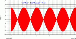
The (radical) test signal is 99KHZ + 100KHZ sines with 1/1 ratio ,
at about 64W RMS/8R for slew induced distorsion evaluation as well
as a THD sim with a single 100KHZ signal at the same power to check
if low HD does correlate with low IMD.
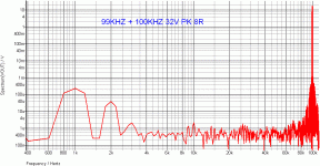
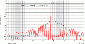
The 99+100KHZ fourier analysis graph is presented in three plots ,
a global linear view , a log scale to highlight the low frequency products
and a restriction to show the high frequency products adjacent to the test
signal frequencies.
It looks like that even at such high frequencies this amp still manage
to work in HiFi territory..
by TIM/DIM/SID/TID , that is , that s all the names given to some
kind of Loch Ness monster that is periodicaly agitating the audio
people cercles still unabated after 40 years or so of a deafs debate...
The (radical) test signal is 99KHZ + 100KHZ sines with 1/1 ratio ,
at about 64W RMS/8R for slew induced distorsion evaluation as well
as a THD sim with a single 100KHZ signal at the same power to check
if low HD does correlate with low IMD.
The 99+100KHZ fourier analysis graph is presented in three plots ,
a global linear view , a log scale to highlight the low frequency products
and a restriction to show the high frequency products adjacent to the test
signal frequencies.
It looks like that even at such high frequencies this amp still manage
to work in HiFi territory..
Attachments
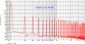
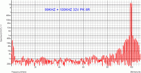
Please confirm I am reading the vertical scales correctly.
In pic 1, the 2nd and 3rd harmonics are about -70dB ref the test tone.
in pic 3, the 1kHz is ~-100dB and the 2kHz is ~-115db ref the test tone
When two tones exist, as in th IMD plots, should we sum the tones for test tone reference voltage?
In pic 1, the 2nd and 3rd harmonics are about -70dB ref the test tone.
in pic 3, the 1kHz is ~-100dB and the 2kHz is ~-115db ref the test tone
When two tones exist, as in th IMD plots, should we sum the tones for test tone reference voltage?
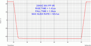
The step response as a complement.
Since the max slew rate is 50V/us it is just obvious that very high
slew rates are not necessary for high perfs in respect of IMD since
any additionnal speed will be perfectly useless as a circuit linearity
becomes the limiting factor once the slew rate is enough for the
projected bandwith reproduction.
Attachments
I had a whole bunch of Hitachi application notes on audio amps using their LatFET's. I'll search them out and put up a copy on the forum. I got them around 1981.
There s tons of derivatives of all kind but the general trend
seems to be picking up the basic app notes at face value,
so it would be interesting to see some of their ideas , for the record..
Check connections of C12 please
Hi Loek,
Please check if it's ok now , I only use PAINT to modify it. Thanks.
Best regards,
Junie

- Home
- Amplifiers
- Solid State
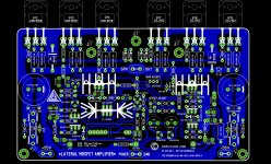
- All Hitachi Lateral Fet amplifier for DIY described by Paul Kemble