Congratulations on a really nice layout. I'd order one, but I am using multiple devices and I already have voltage references and pots with different footprints than those here.

Final board layout isn't fixed in stone yet. There are subtle differences from what's posted... it will support multiple devices (off-board), and has potentiometer fooprints like below. Send me an email pronto if you'd like to get in on the Beta order before it goes out!
Attachments
I was under the impression that the compenstaion cap in parallel with the feedback resistor was something good to have and that its effect was readily visible in the square wave response.
Now this symbol by the master himself suggest something different...
On the other hand the layout traces could have some parasitic pF here and there.
Now this symbol
by the master himself suggest something different... On the other hand the layout traces could have some parasitic pF here and there.
I was under the impression that the compenstaion cap
from Mr. Pass:
"You want to be flexible with compensation cap values."
"I recommend having the holes there, but don't be too eager to fill them..."
I guess that his a pretty clear message that experimentation is advised.
Fred
from Mr. Pass:
"You want to be flexible with compensation cap values."
"I recommend having the holes there, but don't be too eager to fill them..."
I guess that his a pretty clear message that experimentation is advised.
Fred


message to Gina:
I have received your board request, and I've sent two replies to your messages. I'm not sure why you aren't receiving them, but please double-check that you've got your email address set correctly in your diyAudio.com preferences (user cp)... my replies can only go to whatever address you've got in there! You may also want to enable the email option so forum members can contact you. Right now you've got it turned off.
I have received your board request, and I've sent two replies to your messages. I'm not sure why you aren't receiving them, but please double-check that you've got your email address set correctly in your diyAudio.com preferences (user cp)... my replies can only go to whatever address you've got in there! You may also want to enable the email option so forum members can contact you. Right now you've got it turned off.
hifiZen
Thanks. I have taken your advice but that still doesn't resolve the problem I mentioned in my email to you.
Thanks. I have taken your advice but that still doesn't resolve the problem I mentioned in my email to you.
OK, just wanted to inform all our Beta board purchasers that the final board count was 30, at $18.73 per board. 🙂 That doesn't include shipping from the fab house to me, but I'll know the exact total as soon as I receive the invoice.
In about two weeks, grataku and I will begin serious work on rev1.0, and I'll be sending out an email to everyone who's requested rev1.0 boards.
In about two weeks, grataku and I will begin serious work on rev1.0, and I'll be sending out an email to everyone who's requested rev1.0 boards.
Update!
Beta:
Final cost after shipping from fab house was $19.67 per board. At this moment, they are en-route to me via UPS, but won't arrive till Monday (so much for "2nd day" air service!). That means Tuesday I will repackage and ship.
Rev 1.0:
Orders are now at about 120. Price estimate is about $9.50 per board, including the shipping from fab house to me. I've tentatively scheduled production for second week of December, which would mean they'd be shipped out to everyone before December 23rd. Note that I'll be away for an extended vacation until January 13th, so anyone who wants me to delay their order shipment till after Christmas will probably have to wait until mid January, unless I can make other arrangements wrt shipping. I'll be closing orders on rev1.0 boards soon (order closing will be 5:00pm PST, Nov. 26th) and sending out information to everyone to start collecting payments. There's still time to get in on this order, but I want to freeze the quantity so that the costs are fixed. I will order some spare boards, and those who submit a request after I've closed the order will go on a FIFO (first come, first served) list for spare boards / unclaimed boards.
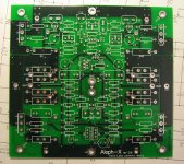
Here are the final versions of the Beta schematics, bill of materials, and board layout preview generated from the gerber files.
rev0.9 schematic
rev0.9 layout snapshot
rev0.9 bill of materials
These are hosted from a private server on a DSL line, so please try to limit your downloads of these files. Thanks.
rev0.9 schematic
rev0.9 layout snapshot
rev0.9 bill of materials
These are hosted from a private server on a DSL line, so please try to limit your downloads of these files. Thanks.
You'll notice that I've provided a number of pads labelled "EXT" on the board. These are there to allow connection of off-board power transistor pairs. I'll provide a proper schematic at some point, but for now, please refer to the Aleph 60 service manual for a diagram showing how multiple output transistors should be connected. Note that the current sense connections only go to one transistor pair on each side of the Aleph-X. These connections must be taken from either the empty pad where Q1/2/10/11 would be installed, or the on-board power transistors should be installed in addition to the external transistors.
Beta testers: I'd appreciate feedback on this feature, and what you think could be done to improve the layout etc, so if you use more than the standard 4 power transistors, please provide me with some notes of your experiences hooking up to the EXT connections.
Beta testers: I'd appreciate feedback on this feature, and what you think could be done to improve the layout etc, so if you use more than the standard 4 power transistors, please provide me with some notes of your experiences hooking up to the EXT connections.
till:
I've tried sending you a reply, but the messages keep getting bounced back to me. Can you please double-check your email address registered on this website? It may be a simple error which is preventing the messages from getting through.
I've tried sending you a reply, but the messages keep getting bounced back to me. Can you please double-check your email address registered on this website? It may be a simple error which is preventing the messages from getting through.
beautiful job Chad/grataku
First rate work, I'm looking forward to hearing the improvements.
John
First rate work, I'm looking forward to hearing the improvements.
John
Very nice design inded.
But are there any reasons for placing the traces for C3 C5 C13 C9 and C10 on the top layer. They will become extremly hard to solder from this side. Even if a PCB is through plated, I like to solder components direct to its traces.
Claus
But are there any reasons for placing the traces for C3 C5 C13 C9 and C10 on the top layer. They will become extremly hard to solder from this side. Even if a PCB is through plated, I like to solder components direct to its traces.
Claus
"They will become extremly hard to solder from this side. Even if a PCB is through plated, I like to solder components direct to its traces."
Uh? I have no idea of what you mean by direct to its traces. In any event the traces for c3 and 5 are on both sides. For the remaining caps I don't remember. The traces and the thru holes are 2 oz of Cu plenty of material to make everyone happy.
Uh? I have no idea of what you mean by direct to its traces. In any event the traces for c3 and 5 are on both sides. For the remaining caps I don't remember. The traces and the thru holes are 2 oz of Cu plenty of material to make everyone happy.
Sorry not traces but tracks,
One rev0.9 layout snapshot posted by HifiZen I see only Red tracks (normally top layer) connecting this components. if there is a malfunction in one the through platings, you have to solder on the top layer side to get a connection, and this is very difficult on components with radial footprints like C3,5 and 13.
Claus
I still don't see your point, the beauty of two or more layers is that traces can run independently from top to bottom, if you require direct soldering to the traces then you limit yourself to single layer.
I am almost hoping for a manifacturing error like that. It would mean free boards. Unfortunately, that never happened to me and I doubt it will in this case.
I am almost hoping for a manifacturing error like that. It would mean free boards. Unfortunately, that never happened to me and I doubt it will in this case.
OK, folks. I received the Beta boards this afternoon, and they look very nice. I'll post a photo for everyone when I get home from work. I will ship tomorrow morning. 😎
- Status
- Not open for further replies.
- Home
- Amplifiers
- Pass Labs
- Aleph-X Official PCB rev Beta & 1.0