

ticktock said:


pssst !! .
gimme back my avatar!
ya don't have anything EMT in signature !!

chinsettawong said:Hello!
I am new to this forum and I am very interested in building this Aleph J. As I cannot find any article or information leading to this Aleph J design, can someone please point me to where I can find the related article, if there is any?
Thanks.
Wachara C.
www.firstwatt.com
this thread
almost every Aleph related thread
Babelfish thread (if you like to laugh)
etc.
chinsettawong said:Hello!
I am new to this forum and I am very interested in building this Aleph J. As I cannot find any article or information leading to this Aleph J design, can someone please point me to where I can find the related article, if there is any?
Thanks.
Wachara C.
Write a nice love letter to Papa . . . !

chinsettawong said:That will keep me busy reading for a while.
Or, read out www.passdiy.com Zen Variations Part2 . . . !
mach.88 said:...one might argue, some people could use 2 sets of ampchannels in one cabinet.
That is two powersuplies sucking at the same time. Limiting the inrush doesn´t seem too far off to me.
Just use one switch for each transformer
... and place them a few centimeters apart to avoid pressing them at once with that big fat thumbJust use one switch for each transformer
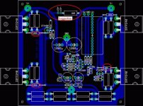
Just a couple of suggestions for the PCB.
Move the 3 resistors circled in red farther away from the solder pads they cross, similar to the same resistor at the top right.
See the suggested layout for the LED and resistor placement change made in this mock-up.
-David
Move the 3 resistors circled in red farther away from the solder pads they cross, similar to the same resistor at the top right.
See the suggested layout for the LED and resistor placement change made in this mock-up.
-David
Attachments
Thx Dave for taking care.
Done as you proposed, and added that "if you want to, you can add a trim pot to R8 / R27 and, after fiddling out the correct value, you may replace it with a fixed R; if you don't care at all, just solder those yellow jumpers"-feature:
Done as you proposed, and added that "if you want to, you can add a trim pot to R8 / R27 and, after fiddling out the correct value, you may replace it with a fixed R; if you don't care at all, just solder those yellow jumpers"-feature:
An externally hosted image should be here but it was not working when we last tested it.
An externally hosted image should be here but it was not working when we last tested it.
Hi Holger,
Nice work so far. Of course we have to have the "Steeno" multi-cap option for C1, that was recently added.
Could we see a version without the silk screen or components in place? It would be nice to see the gaps between the traces and pads.
One other thought is to move the V+ slightly to the left for more clearance.
-David
Dave,
here ya go: http://www.hb001.de/alephjpcbbottom_rc8.pdf
Drill sizes minmized, easier for homemade pcbs.
here ya go: http://www.hb001.de/alephjpcbbottom_rc8.pdf
Drill sizes minmized, easier for homemade pcbs.
Clearance is above 8 mil everywhere, this is what most board houses ask.It would be nice to see the gaps between the traces and pads.
Not a good idea. Need some space for the pcb mounting studs around the corner holes. Moving the pad to the left might cause a short between V+ and the grounded chassis.One other thought is to move the V+ slightly to the left for more clearance.
Mit der jeder das tun kann, was er will
An additional Lochchen under R4 would be nice to allow for 10mm specimens.
(provided you're not sending Christian to Buerklin to get some 6mm 0.6W/TK25 Yageo's)
For DIY picoFarad squeezers :LC
chinsettawong said:Hello!
I notice that there will be 4 mosfets per channel in this set up. Do these mosfets need to be matched?
Wachara C.
yup:
upper two are pair
lower two are pair
ticktock said:Will 500 VA be harmful ??
Yes, but harmful only for your money pocket.
- Home
- Amplifiers
- Pass Labs
- Aleph J Schematic