It's obvious what to do, I'm just making the point that the DIY store boards need a bit more advice for the novices.
golden rule, again :
when in doubt, see original FW schematic
golden rule, again :
when in doubt, see original FW schematic

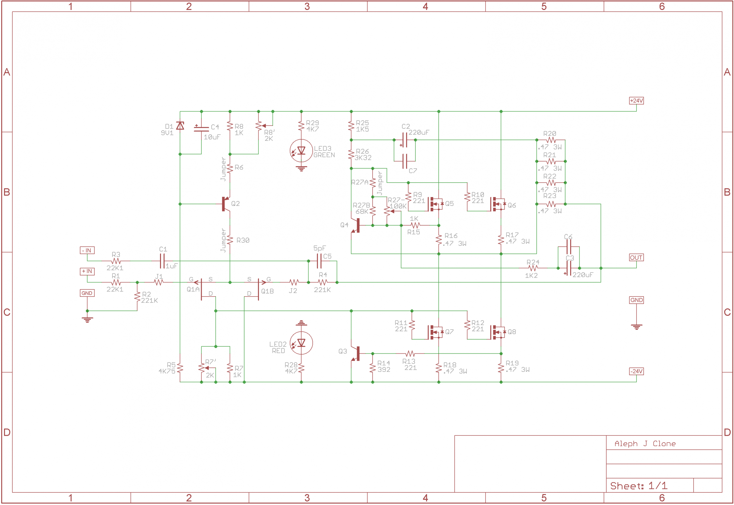
Jumper R6, make R8 resistor 1K, leave R8 potentiometer open to make it closest to original schematic.
Last edited:
There is actually nothing wrong with the DIY store PCB and BOM. R6 and VR8 in combination give approximately 1K. It is just confusing reading the above posts where it is suggested that VR8 be replaced by R8 = 1K0.
I have replaced VR8 (500R) with R8 (1K0). I have also replaced R6 (562R) with R6 (0R0).
I have replaced VR8 (500R) with R8 (1K0). I have also replaced R6 (562R) with R6 (0R0).
I applied this mod to my Aleph J today (10 ohm resistors) and the hum is completely imperceptible on my Klipschorns - inky black background. Thanks! 
I had a bit of time to play with this faint buzz this Australia Day long weekend... so I tried few things. I moved the speaker return from the amp PCB to the power supply PCB. No change. Pretty much anything I did made no change whatsoever...
And then I decided to use my 600-ohm headphones connected straight to the speaker binding posts to be able to hear this faint buzz better while playing with grounding. Well, the headphones made this buzz really audible, so I knew right there and at that very moment what the problem was.... and reached for a Stanley knife and a 9-ohm resistor, in it went between speaker ground and signal ground on amp PCB. Buzz gone, me very happy... amp absolutely dead quiet... like it's not ON.
I also tried feeding the input signal to -IN... and didn't like it.
I applied this mod to my Aleph J today (10 ohm resistors) and the hum is completely imperceptible on my Klipschorns - inky black background. Thanks!
Nice!!!
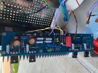
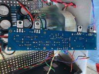
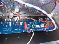
Dear all, my right channel assembly seems to have issues.
I am using paired JFETs from AudioStore
matched MOSFETs from DiyAudioStore - AlephJ transistor kit
For reference I have the following reading compared to my left channel
L channel
R7 - 5.07V
R8 - 8.6V
across Zener- 9.1V
bias 0.5V
Offset - 0.03mV
R7 - 4.07 - does not go above 4.6V in any case, then offset is -13V
R8 - 8.6V
across zener - 9.1V
bias - 0.4V
Offset - 2V
I am not able to fix the offset....it just crazyly moves from + to - and easily reach more than 15V either way.
I double checked the values of resistors, could not find any mistakes, aa jumpers are in...R8 is 1K.
Bias is very stable, but not Offset,
Please suggest what other values to check
Your R channel output stage is "floating", most likely <- the voltage drop across R7 is not sufficient enough to open the MOSFET's.
How did you measure the output bias? Can you re-measure carefully, compare with a good channel, and post the results here.
If everything looks good, values are correct, soldering is sound, no solder bridges, transistor orientation is correct... you may have damaged the input JFET's. Did you ground yourself, did you use an anti-static strap?
Last edited:
Your R channel output stage is "floating", most likely <- the voltage drop across R7 is not sufficient enough to open the MOSFET's.
How did you measure the output bias? Can you re-measure carefully, compare with a good channel, and post the results here.
If everything looks good, values are correct, soldering is sound, no solder bridges, transistor orientation is correct... you may have damaged the input JFET's. Did you ground yourself, did you use an anti-static strap?
Output bias was measured on R18...the results I shared were are comparison on the working channel (L)
Let me test the JFET's, and respond
Unfortunately, you can not "measure" the JFET's.... you can only check if they are shorted... which is not the case with your build.
So, if the bias is correct (I still suggest you re-measure it, just to be safe..), do another visual check of the PCB, soldering, transistor orientation.... (I found one of the Dale resistors to have a different resistance from what its label was saying!!)
Once all the above is done, try a fresh JFET pair - just be sure you are not carrying any static potential, i.e. discharge your body and use the antistatic wristband.
You could also build the bulb thingy (the one that would burn the current in case of a serious short). Then, you could load the output with something like 200-300 ohms resistor / 50 (or 100)W. This would "flash-out" the issue, but the risk to your module starting to smoke in case of something serious.... would also go up.
I was running this by Jim and he hinted (Jim, I hope that was a hint) that I post my problem here, so...
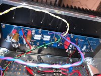
I'm having a similar problem to kpsthakur. I can adjust the offset on the good (left) side to 0. When I try to adjust the bad (right) side nothing happens and I have a static voltage of approximately -21.45 v. On the good board I can adjust the bias to 350 mv. On the bad side I can adjust the bias to 350 mv. So the problem appears to be related to the offset is some way.
I've checked the values of the parts and everything appears to have the correct orientation and location. Photos are attached. Any suggestions?
Attachments
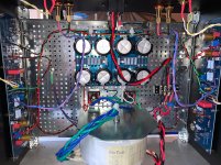
dual mono grounding
have seen different ways that people execute grounding on single chassis dual psu builds. Generally into two camps;
1. IEC earth, both PSU Grounds (w\ CL-60), and both transformer shields on one star
2. IEC earth, one PSU Ground (w\CL-60), and transformer shield from same PSU channel on one star and the other PSU & transformer shield on another star
Is either of these likely to be better than the other from a hum or otherwise perspective?
Would it make any sense to do the following instead?
IEC earth to it's own point, as short as possible.
One PSU Ground (w\CL-60) and that same channel transformer shield to one star and another star of the same for the other channel.
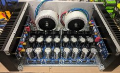
Whatever i do i'm going to have to be a little creative with doing this all inside a 4U with the full diode rectifier boards attached. Things are pretty cozy! Getting close though, maybe next weekend will have everything done. Waiting on a couple of things to show up and hoping to post the full build sometime afterwards.
have seen different ways that people execute grounding on single chassis dual psu builds. Generally into two camps;
1. IEC earth, both PSU Grounds (w\ CL-60), and both transformer shields on one star
2. IEC earth, one PSU Ground (w\CL-60), and transformer shield from same PSU channel on one star and the other PSU & transformer shield on another star
Is either of these likely to be better than the other from a hum or otherwise perspective?
Would it make any sense to do the following instead?
IEC earth to it's own point, as short as possible.
One PSU Ground (w\CL-60) and that same channel transformer shield to one star and another star of the same for the other channel.
Whatever i do i'm going to have to be a little creative with doing this all inside a 4U with the full diode rectifier boards attached. Things are pretty cozy! Getting close though, maybe next weekend will have everything done. Waiting on a couple of things to show up and hoping to post the full build sometime afterwards.
Attachments
- Home
- Amplifiers
- Pass Labs
- Aleph J illustrated build guide