jacco vermeulen said:You're starting to sound like the Self quoting whip.
kwayzee dutchie ;
that's because ya're absent
z1,z2,z3,z4
Looking at the picture in post 88 and considering:
(ref a2serv0.pdf, original service manual)
-You used the protective zeners z1..z4.
-You are testing with unbalanced input
-You did not connect -IN to ground during testing.
-You heard a pop
I would check the input zeners, especially z1 or z3.
I ran a sim to check my suspicion (z1 shorted) and the result is
very similar to your picture in post 88.
You could even consider removing the protective zeners
temporarly and test. Make sure you do connect all equipment
before power on of the amp.
regards
PS
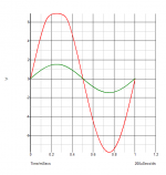
In graph
Green is input 1.5Vp
Red is output
Looking at the picture in post 88 and considering:
(ref a2serv0.pdf, original service manual)
-You used the protective zeners z1..z4.
-You are testing with unbalanced input
-You did not connect -IN to ground during testing.
-You heard a pop
I would check the input zeners, especially z1 or z3.
I ran a sim to check my suspicion (z1 shorted) and the result is
very similar to your picture in post 88.
You could even consider removing the protective zeners
temporarly and test. Make sure you do connect all equipment
before power on of the amp.
regards
PS
In graph
Green is input 1.5Vp
Red is output
Attachments
Re: Re: Re: Low Frequency settle
R19 is now around 80k. --> I_CCS = 500mA
Changing R11 doesn't change zero offset, but it's down to 50mV now
Clipping is still there when input exceeds 600mV or so.
Y'know, by now I have checked, measured and/or replaced almost every component on this PCB. There really aren't that many, and still the behaviour remains.
I'm going to leave it at this, and tomorrow I will bring in the Front end PCB of the still working amp. That way I'll have some comparison.
Zen Mod said:
first - correct R19 that you have Papa's values of Iq ......... 0,5A per each mosfet
fiddle with R11 in same time to preserve zero offset on output
then check AC gain
R19 is now around 80k. --> I_CCS = 500mA
Changing R11 doesn't change zero offset, but it's down to 50mV now
Clipping is still there when input exceeds 600mV or so.
Y'know, by now I have checked, measured and/or replaced almost every component on this PCB. There really aren't that many, and still the behaviour remains.
I'm going to leave it at this, and tomorrow I will bring in the Front end PCB of the still working amp. That way I'll have some comparison.
Attachments
Re: z1,z2,z3,z4
Z1 - Z4 were one of my first suspects... Quite right, especially because clipping starts when the unbalanced input exceeds 0.6V.. precisely one PN junction.
However, I have removed Z1 and Z3 in post 74, and they haven't been back ever since...
rtirion said:Looking at the picture in post 88 and considering:
(ref a2serv0.pdf, original service manual)
-You used the protective zeners z1..z4.
-You are testing with unbalanced input
-You did not connect -IN to ground during testing.
-You heard a pop
I would check the input zeners, especially z1 or z3.
I ran a sim to check my suspicion (z1 shorted) and the result is
very similar to your picture in post 88.
You could even consider removing the protective zeners
temporarly and test. Make sure you do connect all equipment
before power on of the amp.
regards
PS
In graph
Green is input 1.5Vp
Red is output
Z1 - Z4 were one of my first suspects... Quite right, especially because clipping starts when the unbalanced input exceeds 0.6V.. precisely one PN junction.
However, I have removed Z1 and Z3 in post 74, and they haven't been back ever since...
Bakmeel said:No. I didn't.
Grounding actually worsens the problem. Clipping then starts at 300mVp-p input.
-edit-
But why ground -IN? there is a parallel 10k to ground there? (R5)
you're right ;
R5 is there as foolproof part
I didn't know did you installed it or not .
did you checked all resistor values ..... ?
Zen Mod said:in that case ..... if you are sure that all semis and passives are 100% OK ....... your conformal coating or something else ...... dreked your pcb
pull out pcb from other channel ..... and measure everything (passively-with DMM), comparing good and bad channel
I share same opinion how to find defected device....or PCB? I mentioned here several times check PCB if paths are conductive...(according pictures it looks that you painted boards from solder side...Am I right?)


testbench
Your sim circ probably has only 0,3 .. 0,5 A bias.
Because of one output pair only, and no adjustments to
source resistors.
Guess what happens in a 10Ohm load looking at voltage only?
Clipping at 6V .. 10V.
Not a fair comparison to your real amp.
My aleph 2 sim confirms inputvoltage tolerance of 4Vp (8Vp-p)
unbalanced, U-IN not connected and nearly 40Vp output at 3 amp
bias in 8Ohm resistive load.
Clipping starts at around 4.2Vp Input
This is sim only. I have found measurements on an actual Aleph 3
and sims of the Aleph 3 to be nearly the same. I have no reason
to believe an Aleph 2 to behave differently.
Hope this helps.
Re: testbench
Quite right... The sim is (should be) representing the test bench I have here in the lab... And they seem to agree on the clipping...
Simming the entire amp gives completely different results yes... So now I have to take back this board to my own little workshop and integrate it back into the beast.... Likely that it will be purrin' like a little kitten again...
Frustrating discovery... but a good one to.... heh..
rtirion said:Your sim circ probably has only 0,3 .. 0,5 A bias.
Because of one output pair only, and no adjustments to
source resistors.
Guess what happens in a 10Ohm load looking at voltage only?
Clipping at 6V .. 10V.
Not a fair comparison to your real amp.
Quite right... The sim is (should be) representing the test bench I have here in the lab... And they seem to agree on the clipping...
Simming the entire amp gives completely different results yes... So now I have to take back this board to my own little workshop and integrate it back into the beast.... Likely that it will be purrin' like a little kitten again...
Frustrating discovery... but a good one to.... heh..
Preliminary tests
Well, actually I'm on the birthday of my little niece right now...
Yesterday night I intergrated the "faulty" PCB back into the main amp and ran it for about 2,5 hours on a resistor load. Performance seems nominal so far.... Tomorrow I'm going to do a full day burn-in trial on the resistor load.
To be continued....
Break-in test
G'day y'all...
So today I'm doing a break-in test. I've switched on the amps around 13:00 CET today, and it is now 15:15 CET, so the amps have been running for about 2 hours now. Here is a few numbers on performance while the amps are in idle (no signal input):
Left Channel (Amp #1)
DC offset on speaker terminals: -45mV
V_R11 = 5.27V --> 23.8mA
V_R14 = 4.14V --> 10.5mA
V_Q3gs = 3.85V
V_R40 = 353mV
V_R46 = 358mV
V_Q6-Q11 = 4.14V
V_Q12-Q17 = 4.14V
Right Channel (Amp #2, the "repaired" one)
DC offset on speaker terminals: -18mV
V_R11 = 5.32V --> 24.0mA
V_R14 = 4.16V --> 10.6mA
V_Q3gs = 3.85V
V_R40 = 365mV
V_R46 = 360mV
V_Q6-Q11 = 4.20V
V_Q12-Q17 = 4.16V
To me all values seem to be in good order. There are small differences, but IMHO within nominal tolerances. In fact, looking at the DC offset alone, the "repaired" amp seems to be slightly better than the "original" one... note that I changed all components back to the originally selected ones except Z1-Z4 which I destroyed when taking them out.
Last friday night, I checked the full power performance. Clipping starts at 4.5V / 5.2V depending on frequency. The lower the frequency, the more power I can get. Clipping is symmetrical.
What happened?
That's probably going to remain a mystery... Honestly, I have checked every single component.. in-circuit, some of them out-circuit and all of them are fine. I have only a hunge on what might have happened, but I can't support my theory with manufacturer data:
Sometimes, electrolytic capacitors can experience a small break-down between the aluminium layers, through the wet electrolyte. In some cases, this breakdown is self-healing as the electrolyte quickly flows into the small hole burnt in the aluminium. During this time, the capacitor experiences a temporal increase in its leakage current, while it behaves as a very bad and noisy resistor. If C5, C9 or C10 would have experienced such a minor breakdown, this would explain the pop-and-hiss sound I heard... Simply because these caps are in the signal path.
If this is what really happened? I don't know.... any other theory is welcome
-- edit--
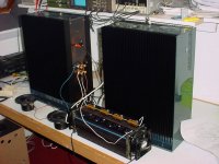
Picture from the amps under test....
G'day y'all...
So today I'm doing a break-in test. I've switched on the amps around 13:00 CET today, and it is now 15:15 CET, so the amps have been running for about 2 hours now. Here is a few numbers on performance while the amps are in idle (no signal input):
Left Channel (Amp #1)
DC offset on speaker terminals: -45mV
V_R11 = 5.27V --> 23.8mA
V_R14 = 4.14V --> 10.5mA
V_Q3gs = 3.85V
V_R40 = 353mV
V_R46 = 358mV
V_Q6-Q11 = 4.14V
V_Q12-Q17 = 4.14V
Right Channel (Amp #2, the "repaired" one)
DC offset on speaker terminals: -18mV
V_R11 = 5.32V --> 24.0mA
V_R14 = 4.16V --> 10.6mA
V_Q3gs = 3.85V
V_R40 = 365mV
V_R46 = 360mV
V_Q6-Q11 = 4.20V
V_Q12-Q17 = 4.16V
To me all values seem to be in good order. There are small differences, but IMHO within nominal tolerances. In fact, looking at the DC offset alone, the "repaired" amp seems to be slightly better than the "original" one... note that I changed all components back to the originally selected ones except Z1-Z4 which I destroyed when taking them out.
Last friday night, I checked the full power performance. Clipping starts at 4.5V / 5.2V depending on frequency. The lower the frequency, the more power I can get. Clipping is symmetrical.
What happened?
That's probably going to remain a mystery... Honestly, I have checked every single component.. in-circuit, some of them out-circuit and all of them are fine. I have only a hunge on what might have happened, but I can't support my theory with manufacturer data:
Sometimes, electrolytic capacitors can experience a small break-down between the aluminium layers, through the wet electrolyte. In some cases, this breakdown is self-healing as the electrolyte quickly flows into the small hole burnt in the aluminium. During this time, the capacitor experiences a temporal increase in its leakage current, while it behaves as a very bad and noisy resistor. If C5, C9 or C10 would have experienced such a minor breakdown, this would explain the pop-and-hiss sound I heard... Simply because these caps are in the signal path.
If this is what really happened? I don't know.... any other theory is welcome
-- edit--
Picture from the amps under test....
Attachments
- Status
- This old topic is closed. If you want to reopen this topic, contact a moderator using the "Report Post" button.
- Home
- Amplifiers
- Pass Labs
- Aleph 2 - The Final Build