
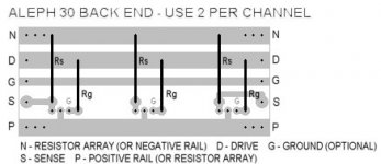
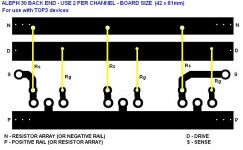
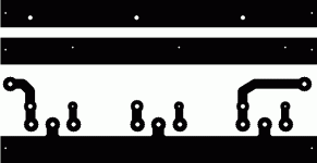
Aleph 30 back end
Here comes layout for the Aleph 30 output stage. Use this one if you have mosfets with TOP3 (TO247) package for example IRFP240. The layout posted above is for TO-220.
/Freddie
(I just did some changes to the layout, the holes were too big)
Here comes layout for the Aleph 30 output stage. Use this one if you have mosfets with TOP3 (TO247) package for example IRFP240. The layout posted above is for TO-220.
/Freddie
(I just did some changes to the layout, the holes were too big)
Attachments
Grey,
I just finished making the layout for my Aleph 5 using yours as a starting point (thank you very much). I opted for double sided prints with a ground plane (saves etching fluid.........), using one eurocard (100x160mm) for two front end boards and one eurocard for four output boards. The advantage with euroboards is that you can get them with a thicker copper layer (70 mu).
There´s one thing I didn´t understand in your layout, the "from output devices (CS sence)" is used twice. Why didn´t you connect the emitter from Q5 with "from output devices" on the print itself?
And another question: What´s the advantage of R0? It´s used with the 60 but not with the Aleph 5 or 4.
william
William,
Since you're using a double-sided board, you can run the emitter of Q5 on the other side of the board. I set myself the task of making a single-sided Aleph board. I have nothing against double-sided PC boards, and in fact usually keep some around, but I found that I didn't really need it for this project.
If you think you see a way to sneak a trace from the emitter of Q5 around to the top of the resistor array, by all means do so. However, if you're using a double-sided board, a larger board, or run a connection to the interior of the board (instead of connecting at the edge), you've changed the rules of the game.
To me, doing a PCB layout is like assembling a jigsaw puzzle. I don't have any fancy software; I do the layouts by hand, trying several different versions, then keeping the best portions of each. It's a nice mental challenge. My goals are:
--No interior connections.
--Keep connections to as few edges of the board as possible. This isn't really strictly necessary, but it makes service easier if you can unbolt the board and get underneath while it's still connected. In this case, I managed to keep connections down to three sides, one side exclusively inputs, with no high current wires nearby.
--Keep signal traces as short as possible.
--Keep the overall board as compact as possible, while allowing for heat dissipation. I cut my boards to size on a band saw. If you want to use a larger board, then other options might present themselves.
--Use as few layers as possible.
--No jumpers allowed.
--To the extent possible, keep components lined up. This is purely esthetic--it makes my eyes happy to see nice orderly rows like that. I was particularly smug when I managed to get that long row together across the middle of the board. Not that it matters to anyone but me. Bear in mind that at the time that I did the layout, I hadn't really considered that anyone else would ever see the layout but me. As far as I knew, there were only two homebrew Alephs in the world, mine and Mark Finnis's. It never entered my mind that there would be so many other folks who would take on the building of an Aleph, or that I would be posting my layout online. I just did as neat a layout as I could imagine and went on from there.
Note that large regulated power supplies generally run an output and a separate voltage sense. The sense connection is connected to the load with a light gauge wire, as there's no current draw to speak of and hence no voltage drop across the wire. In this manner the sense/feedback circuit within the power supply is able to get an accurate reading of what's going on at the load without having to worry about heavy losses across the output cable.
That's similar to what I did with the Aleph layout. A fairly heavy wire (I forget what I used, 12 ga. maybe? doesn't really matter, it's only about 2" long) for the actual output, and a much smaller wire (about 20 or 22 ga.) for the sense.
The purpose of R0 (along with R1 & R8, which I opted not to use) has been covered before. R0 is there to keep ground loops from forming. You can omit it and jumper straight to ground if you like.
Grey
First off, I would like to thank everyone who has contributed to this forum. I recently joined and have enjoyed reading everyone's posts. I was wondering if anyone could lead me to the schematic for the board layout that is posted on this thread. I have all the schematics from the passdiy website (aleph 2, 3, 4, 5) but can't seem to get all the reference designators to match with the layout that is posted. I see mentions of the volksamp schematics, are those available?? I and a co-worker of mine are in the process of planning the construction of two aleph4 amplifiers and may be interested in using this layout. Also, I missed the explaination of why R0 (R1, R8?) helps with ground loops. Can anyone help me with this? I do not see how an additional resistor from R4 and R5 to ground can help. aren't they already tied to ground? Thanks for your help.
Jake
Jake
Jake,
The Aleph amplifiers began life as a product in the Pass Labs lineup, lived a long (by audio standards) and fruitful life, then passed into the great listening room in the sky.
But...
The stereo gods had mercy and, due to the great diligence and valor shown during their first life, granted the Alephs a second life under the moniker Volksamp (www.volksamp.com). Two circuits were chosen for this special priviledge, the Aleph 2 and the Aleph 3.
However, both were returned to life with some differences. Lower bias current in the output stages--this so that the smaller heatsinks would not be overburdened--and a bit of a re-fiddled front end.
After rolling the bones and swirling tea leaves, I decided to use portions of the newer front end design, but mostly the older circuit of the Aleph 2. After adding the resistors for the front end, the resistor numbering became problematic, so I simply defaulted to the Volksamp numbering scheme for the rest of the parts. This should all become somewhat clearer when you look at the Aleph 60 schematic.
There's a thread somewhere back in the Pass Labs forum where Nelson addressed the R0, R1, and R8 issue. None of them are necessary. R0, as stated above, is for ground loop prevention. R1 & R8 are for DC balance and CMRR, and are selected to match the transistors that are actually in the circuit.
Grey
zener current
Hi folks, I'm the new guy. An Aleph 4 is my first and only electronics project. I'd like to participate in this forum by shareing my subjective conclusions as they relate to the value of R13.
When I first completed my Aleph the sound albiet good was not quite the warm and romantic sound I was expecting. I trusted my subjective conclusions enough to decide an some aspect(s) of my version was not up to factory par.
I read the A75 articles on the Passlabs site and drew the conclusion the 1 watt zener I was using for Z9 should have been a 1/2 watt type and perhaps 4 ma of current through it wasn't enough to keep it quiet. I didn't have any 1/2 watt zeners around so I played with the value of R1. With R1 changed from 10K to 6.8K the sound was now darker and less hard, a decided improvement.
I bought some 1/2 zeners and replaced the 1 watt types at the same time returning R13 to it's orginal 10K value. The sound is better yet, now possessing a wounderful black ambience. For the purposes of experimentation I retried the 6.8K resistors and found I prefered this over the original configuration, yet another small step in the warm/romantic direction. I suggest you try it for your self.
I should also mention I am using tantalum caps on the neg input and maybe they contribute some hardness to the sound. I haven't tried anything else and will gladly entertain suggestions!
I don't want to come across arogent by deviating from Nelson's fantastic design. I don't claim this slight change to be a general improvement, I simply found a way to satisfy my own subjective taste within my given stereo set up . In other words be nice to the new guy!")
Brett
Hi folks, I'm the new guy. An Aleph 4 is my first and only electronics project. I'd like to participate in this forum by shareing my subjective conclusions as they relate to the value of R13.
When I first completed my Aleph the sound albiet good was not quite the warm and romantic sound I was expecting. I trusted my subjective conclusions enough to decide an some aspect(s) of my version was not up to factory par.
I read the A75 articles on the Passlabs site and drew the conclusion the 1 watt zener I was using for Z9 should have been a 1/2 watt type and perhaps 4 ma of current through it wasn't enough to keep it quiet. I didn't have any 1/2 watt zeners around so I played with the value of R1. With R1 changed from 10K to 6.8K the sound was now darker and less hard, a decided improvement.
I bought some 1/2 zeners and replaced the 1 watt types at the same time returning R13 to it's orginal 10K value. The sound is better yet, now possessing a wounderful black ambience. For the purposes of experimentation I retried the 6.8K resistors and found I prefered this over the original configuration, yet another small step in the warm/romantic direction. I suggest you try it for your self.
I should also mention I am using tantalum caps on the neg input and maybe they contribute some hardness to the sound. I haven't tried anything else and will gladly entertain suggestions!
I don't want to come across arogent by deviating from Nelson's fantastic design. I don't claim this slight change to be a general improvement, I simply found a way to satisfy my own subjective taste within my given stereo set up . In other words be nice to the new guy!
Brett
Just a postscript on the fate of the Aleph design. We
have re-acquired the Aleph for the purpose of integrating
it into the XA products at Pass Labs, and I intend to put
newer Alephs onto the market in something resembling
the original and current circuit.
The Volksamp Alephs are terrific products; in my opinion
better performing than the originals, but they have only
enjoyed lackluster sales, and that is, of course, not
acceptable.
Thanks Grey,
That clears up that part. I reviewed the volksamp schematic and some things do not make sense to me:
1) I do not see any dominant pole compensation capacitor. Is this circuit stable without it?
(the other Aleph amps have 680pF or .001)
2) I see that C18 is supposed to get rid of supply ripple, but why isn't it just returned to ground instead of Q5 emitter?? Doesn't the noise go straight through C18 onto the outut rail? I do not see the logic behind this.
3) Also, I have seen C21 from collector to base(Q5) and sometimes from collector to emitter(Q5), what's up with that??
4) one other observation, no thermister in the transformer primary, is inrush current not important anymore??
later
Jake
PCBs for aleph30 and aleph L
PCBs for aleph30 and aleph L
Dear fellow Aleph DIYers, after a popular demand about my aleph PCBs published on Passdiy.com, I decided to publish my designs in jpg format for easy printing .
However I will only do so if if Mr. Nelson Pass grant me the permission to do so.
Note though that these are just scans of my prints as my pcb editor do not output any kind of popular format (the editor i use is board maker by Tsien Labs). However although scans are not perfect, the prints are o.k for fabrication of the pcb. I also include the stuffing diagram in two versions (mask1 & mask2). The parts numbering system is the one used in aleph30.
Moreover, I also made a pcb for the aleph L but i will only publish it after the kind permission of Mr Nelson Pass.
Once more I would like to thank Him personally for being our source of information and knowledge.
Panos
Jake,
1) Stability is a relative term. The Mini-A sitting next to me was behaving poorly. I moved the wire for the negative rail. It became meek and mild-mannered. I haven't had any problems with the Aleph 2.60 circuits.
2) Q5 rides up and down with the output waveform. If you tie C18 to ground, you'll be getting the output waveform across it. Besides, if you think about it, the output rail is a (fairly) low Z path to ground, anyway.
3) Gremlins.
4) Thermistors aren't necessarily called for in the Great Scheme Of Things. If you want a thermistor, put one in. There have been zillions of amps built without them, and will be zillions more before all is said and done. There's a tremendous amount of latitude involved in building circuits. Far more than many people realize. Many part values are chosen because the part happened to be next to one's elbow at the moment when the need arose and it worked. Those who live by numbers, slavishly calculating each and every part to nine decimal places, fail to see the forest--they're too busy counting trees. True, there are numbers that must be adhered to: Don't exceed the ratings of a part, for instance. But people who get flustered over the difference betweent 100,000uF and 120,000uF in the power supply because the formulas tell them that 100,000uF is 'enough' are missing the point.
If you build it, the music will come.
scrazy,
I matched parts out of circuit. If you want to do so in situ, by all means do, but it will save time if you at least rough them in so that you have similar devices grouped together. You could, I suppose, wire up the front end differential by itself and test it. Make sure that Q2's gate is grounded so that it doesn't flop around like a dead fish and cause problems. However, the front end is such a simple thing that there's not much that can go wrong unless you put in one of the MOSFETs backwards.
You wouldn't do that, would you?
DC offset is measured at the output. I'd use a load resistor.
Grey
thanks Grey
Is there "High Resolution" PCB layout image avaliable?
Because "Low Resolution" image's qualtiy is not very good when using them for printing...
As I remember you using IVEX for PCB design, maybe I could using your IVEX pcb files convert to higher resolution image suitable for printing?
thanks again...
The file format that Ivex uses won't upload, as it's BRD, whereas the upload function here only allows GIF, JPG, etc. I'll ponder on this a bit and see what I can come up with. Don't expect instant results, as Geoff and I hammered on this for a week just to get this far.
The long term solution, I fear, will be to recreate the board layout by hand in CIRCAD--which does export BMP files--but that's going to be a real nuisance. Needs to be done, however, as I want that Ivex software off of my computer ASAP.
Grey
The long term solution, I fear, will be to recreate the board layout by hand in CIRCAD--which does export BMP files--but that's going to be a real nuisance. Needs to be done, however, as I want that Ivex software off of my computer ASAP.
Grey
Guys, I'll do what I can, but I've got a virus rampaging through my PC at the moment--kinda like Godzilla tearing into Tokyo--I'll be lucky if I get out of this in one piece.
My stories are my highest priority, gotta rescue them first. I'll try to save the board files and stuff, of course, but those will have to wait their turn...
Grey
My stories are my highest priority, gotta rescue them first. I'll try to save the board files and stuff, of course, but those will have to wait their turn...
Grey
- Status
- This old topic is closed. If you want to reopen this topic, contact a moderator using the "Report Post" button.
- Home
- Amplifiers
- Pass Labs
- Aleph 2 (& others) as a project