I hope I'm working for both of us
Yes... you do so! Problem is, i have to take care of another thing between also
Jesper.
Attachments

The I/V resistor is the "virtual short" seen by the current source (DAC) when it is connected directly to the inverting input of the op-amp. So the op-amp does all the work - you don't need a separate I/V resistor.
What I don't really like about these op-amps is that this "virtual short" is not really a short. For example, the AD844 appears like a ~50R resistor. The OPA860/1 seem to be better (at ~13R if I'm reading the datasheet correctly).
I may be wrong of course, I'm just now trying to go a little deeper on I/V converters due to an ES9038 that I'm thinking about building.
AD811 can provide a dynamic impedance of less than 1 ohm.
The only reason why people use inferior AD844 is because AD811 is difficult to implement and run in a stable fashion. However, it is simply the best I/V solution - definitely worth investigating, especially with a low current-out DAC's.
Member
Joined 2006
With CFP connected transistors You can achieve impedance values down to a few mOhms.
Plus, You can choose the idle currents considerably higher and Your not bound to the typical power supply voltage limits of OPAmps
You have shown a working circuit of such in the past, could you post it again Calvin?
Hi,
both, the AD844 and the AD811 are current feedback OPAmps.
The important difference seems, that the AD844's TZ node is accessible while the AD811s is not.
The accessibility of the TZ node allows to run the AD844 openloop while the AD811 only operates with global feedback.
While this generates nice figures on paper one can debate about the effects of global feedback on sonics.
Beeing a current feedback OPAmp the value of the feedback resistor affects bandwidth and dynamic behaviour which makes the choice of the resistor, hence the level of output voltage a bit critical.
jauu
Calvin
ps. I'll see if I can find the circuit
Hi,
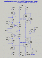
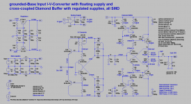
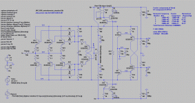
found the principle circuit and a couple of other grounded-base IV stages
Shown inthe first pic is a complementary CFP-Input working on current mirrors with CFP output legs.
Of course can the CM input legs (Q3a/Q4a) be CFPed also.
The third pic is a folded cascode with paralleled input transistors for reduced input-impedance and/or high-current DAC-outputs.
The second pic shows a bipolar IV-stage Sen/Zen-style (after EUVL) with floating supply and bipolar buffer.
The floating supply for the IV-part could be generated from the symmetrical Buffer-Supplies with an DC-DC switcher (with low coupling capacitance ... XP-Power for example)
Attached also is a AES-Paper by Smedegaard (11/1996) that deals with the Q of low input impedance for IV-converters.
jauu
Calvin
Attachments
Hi,
found the principle circuit and a couple of other grounded-base IV stages
Shown inthe first pic is a complementary CFP-Input working on current mirrors with CFP output legs.
Of course can the CM input legs (Q3a/Q4a) be CFPed also.
The third pic is a folded cascode with paralleled input transistors for reduced input-impedance and/or high-current DAC-outputs.
The second pic shows a bipolar IV-stage Sen/Zen-style (after EUVL) with floating supply and bipolar buffer.
The floating supply for the IV-part could be generated from the symmetrical Buffer-Supplies with an DC-DC switcher (with low coupling capacitance ... XP-Power for example)
Attached also is a AES-Paper by Smedegaard (11/1996) that deals with the Q of low input impedance for IV-converters.
jauu
Calvin
Have you checked the AD811?
It performs very well compared to all other solutions shown in that article you attached.
This IC will provide close to 6V pp of output at a very low distortion levels, while keeping the voltage swing at Iout DAC pin well below the compliance threshold, allowing all Iout DACs to perform at their best as well.
The problem with 811 is in its correct implementation, which is quite hard due to its max Vcc/Vee limitation, huge bias, and very fast speed that requires careful layout and parts' selection to prevent oscillations and rise in THD.
Hi,
on paper the AD811 certainly looks better than the usual IV-OPAmp candidates.
At least it is a wide bandwidth, very fast settling OPAmp.
Hawksford wrote a paper on the problem of slow OPAmps as I/V converters and showed that the steep current step-flanks tend to overdrive the OPAs inputs, so that they could run under openloop conditions with associated recovery time and THD.
One typically found measure is to put a cap from the DAC´s output to gnd to ´slow down´ the DAC output.
The Smedegaard paper shows the additional issue of early rising Zin of OPAmps.
jauu
Calvin
Hi,
on paper the AD811 certainly looks better than the usual IV-OPAmp candidates.
At least it is a wide bandwidth, very fast settling OPAmp.
Hawksford wrote a paper on the problem of slow OPAmps as I/V converters and showed that the steep current step-flanks tend to overdrive the OPAs inputs, so that they could run under openloop conditions with associated recovery time and THD.
One typically found measure is to put a cap from the DAC´s output to gnd to ´slow down´ the DAC output.
The Smedegaard paper shows the additional issue of early rising Zin of OPAmps.
jauu
Calvin
Nice teaching, all the schematics Calvin
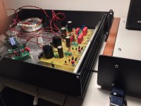
I will read those Smedegaard papers before bedtime today, in meantime i tested my dac for good heat transfer in my new hifi2000 chassis.
I have those four shuntregulators, and they heat up, but i think i managed to cool them enough with 3mm thick alu' bottomplate and some bars connecting the transistors to the chassis-left_side; the sides are aka heatsinks made in nice aluminium too... really nice chassis. -The setup ran for 1-1/2 hour without the alubars getting >40C.
Thanks all... !
Jesper.
Attachments
Hello here!
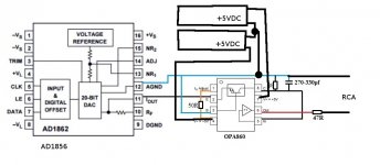
I found another thread, where OPA860 was suggested as i/v stage for the AD1862.
See eventually post #38 in this http://www.diyaudio.com/forums/digital-line-level/299414-i-v-analog-output-stage-ad1862-4.html... Where Calvin is explaining a lot
As i understand the OPA860 is good, when no buffer are used after opamp, and the OPA861 is when one like to roll his own buffer?
Right ?
I have "corrected" the circuit, and maybe i can try this for a start?
It look's like the AD1862 is much like my AD1856, but havent been studying it closely yet through.
Jesper.
Attachments
My old DAC (Monarchy 18b) uses AD811 for I/V (pretty much like Walt Jung's circuit), but the AD844 I/V in NFB fashion just beat it without breaking a sweat.
That simply can't be the case, and here's why... The AD844 smoothed out the harshness coming from the rest of the system... hence you think it is better.
The document calvin uploaded clearly states that AD811 was, in fact, better than anything else suggested in this whole thread.
My experiments also proved that in a 1704 differential AD811 I/V -> to LM6172 differential-to-single-end converter analog stage. But implementation has to be done right, with a stable operation and adequate power supply rail decoupling.
AD811 / LM6172 approach requires the rest of the system to be quite good. Then, the AD811 can actually show what the source is capable of.
Many DYI-ers simply expect AD811 to work without putting in a bit of a hard work, which usually results in AD811 overheating and burning out.
Last edited:
Hi,
connected as current-feedback amp encompassed by a global fb-loop the AD844´s paper performance is inferior to the AD811´s, yes.
The point though is, that the AD844 allows for openloop working, which the AD811 doesn´t.
As the openloop behaviour is not shown or data given (only the static values in the tables) one can´t really compare the performance of the AD811 versus AD844-openloop on paper.
The dynamic performance of the AD844 will differ considerably between openloop and closedloop conditions.
There´s enough local feedback to find in every corner of the current conveyor and diamond buffer stage.
And the Q remains, why should one apply global feedback if it doesn´t improve signal behaviour in a significant way?
In this application it rather creates than solves problems ... not to talk about the sonic misery it often causes ;-)
jauu
Calvin
So i was looking into, how i do the +/- 5vdc supply?
Anyone here have experiance with this sort of regulators?
http://uk.rs-online.com/web/p/isolated-dc-dc-converters/2176698/?searchTerm=217-6698&relevancy-data=636F3D3126696E3D4931384E525353746F636B4E756D6265724D504E266C753D656E266D6D3D6D61746368616C6C26706D3D5E283F69292852537C5253207C52532D293F5C647B337D285C73293F5B5C732D2F255C2E2C5D285C73293F5C647B332C347D2426706F3D313426736E3D592673743D52535F53544F434B5F4E554D4245522677633D4E4F4E45267573743D3231372D36363938267374613D3231373636393826
Jesper.
I would steer clear. It's a switcher with 50mV of ripple..
If I were building an I/V converter I'd power it by a pair of Ref-Ds (like you're contemplating) or by a bipolar Salas BiB.
Hey
It was my plan from scratch, but after asking in the Ref.-D thread i realized that i need another trafo and two more Ref.-D's for making "isolated" +/-5vdc.
That's why i was looking for another solution; but your'e proberly right, there is no easy catch here!
Jesper.
GND connection on line
Hi here.
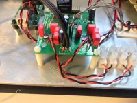
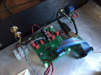
I am in progress of building my little DAC, with the giant's PSU's into a chassis.
But i am i doubt howto connect the GND connection from the DAC to chassis.
I have soldered in two RCA's on the DAC-pcb (See picture), and this setup is working without any hum or noise at all; but i have to attach the GND line from maybee the end of the RCA cables, or is it better i do it at the PCB end? or maybee somewhere else? -Any suggestions?
The DAC is feeded with +/-12vdc in the middle of the pcb, with the grey wires.
Also the DAC is feeded with 3.3vdc (right top on picture) -I think this connection is isolated from the DAC chip themselves, and only used for the "stop-clock"... The last psu is feeding +5vdc into the xmos-pcb.
Hoping someone can tell me a good spot to connect gnd to chassis?
Jesper.
Hi here.
I am in progress of building my little DAC, with the giant's PSU's
into a chassis.But i am i doubt howto connect the GND connection from the DAC to chassis.
I have soldered in two RCA's on the DAC-pcb (See picture), and this setup is working without any hum or noise at all; but i have to attach the GND line from maybee the end of the RCA cables, or is it better i do it at the PCB end? or maybee somewhere else? -Any suggestions?
The DAC is feeded with +/-12vdc in the middle of the pcb, with the grey wires.
Also the DAC is feeded with 3.3vdc (right top on picture) -I think this connection is isolated from the DAC chip themselves, and only used for the "stop-clock"... The last psu is feeding +5vdc into the xmos-pcb.
Hoping someone can tell me a good spot to connect gnd to chassis?
Jesper.
Attachments
But i am i doubt howto connect the GND connection from the DAC to chassis.
I have soldered in two RCA's on the DAC-pcb (See picture), and this setup is working without any hum or noise at all; but i have to attach the GND line from maybee the end of the RCA cables, or is it better i do it at the PCB end? or maybee somewhere else? -Any suggestions?
You'll want to ensure that common-mode currents (carried by your interconnects, both digital and analogue) find their way back to mains earth without passing through sensitive circuit nodes en-route. However you also want the common-mode currents which enter via your transformers' inter-winding capacitance to resolve to earth without passing through sensitive nodes.
Trying to satisfy both gives something of a conundrum - if you resolve the interconnect currents optimally this means a 0V-chassis connection close to where the interconnects enter. However may well mean your transformer currents pass through your PCB to get to chassis which is far from optimal.
Okay... very thoughtfull i must say
I will do as i use to do, namely try different solultions starting with grounding the rca's or maybee none conenction at all! ... Case is i tried that such equipment can give some "static" shocks (not dangerous), even if mains are grounded; thats ofcause due that none of the secundary circuit is not grounded (kindof floating)... but i allways thought that such solutions was bad practice.
Jesper.
Final thermal/heat/stability test
Morning folk's!
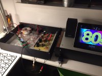
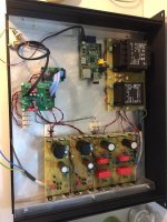
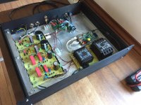
Today i finally got my DAC packed all up in this brandnew hifi2000/modushop chassis.
Going to make some "long"-term test before it is going into my main system.
If one look carefully at the pictures, you can see that i after many hours of struggling with this finally got a USB switch to work proberly. The switch can choose between USB cable input or "internal" RaspberryPi player.
As for the I/V conversion, Calvin has been so kind to calculate and send me some schematic, but it would be some time before i can actually make it through.
*Have a nice day out'there!
Jesper.
Morning folk's!Today i finally got my DAC packed all up in this brandnew hifi2000/modushop chassis.
Going to make some "long"-term test before it is going into my main system.
If one look carefully at the pictures, you can see that i after many hours of struggling with this finally got a USB switch to work proberly. The switch can choose between USB cable input or "internal" RaspberryPi player.
As for the I/V conversion, Calvin has been so kind to calculate and send me some schematic, but it would be some time before i can actually make it through.
*Have a nice day out'there!
Jesper.
Attachments
- Status
- This old topic is closed. If you want to reopen this topic, contact a moderator using the "Report Post" button.
- Home
- Source & Line
- Digital Line Level
- AD1856 I/V (I/U) converter