Hello ")
In my adventure with my new "old" AD1856 R2R ladder DAC, i finally get to listning to a temp. setup here at home. -If someone here had read about my adventures in the Salas SSLV thread you got the idea, me saying adventure. Well i had some minor explosions setting up the power supplys for this little DAC, but most survived through! ... Anyway the DAC and PSU's are all working now.
Me and our oldest (boy 19years), sat down (as usual when pa' got new equipment), and did some listning test.
My current setup is a buildin iqaudio dac, buildin along with an RPI in my Salas DCG3 linestage, so doing A/B test is very easy now.
I started my tidal and my logitech squeezebox interface on my PC; from there i can easily switch between the two dac's (ofcause i also have to switch the input on the DCG3) ... So first number we played i did not tell my son, which dac, was playing; but after 5-10sec. he told me that everything sounded better than everything else he heard. -Which dac? yes the new one was playing ... Well we tested ofcause, and besides some crappy recordings, there was no doubt that this new dac is smoother and less sibiliance-aggresive.
What i donno for now, is how much the Reflector-D's and SSLV's has to do with this smooth and listning richable dac?; but as long as it sound so good i can live with that quistion (for now)...
Okay, back to topic, and why i started this thread at all !
I bought this DAC from diyinhk, and they wrote on theire site, iout is possible.
I have been searching for a I/V circuit to tryout, but i am having trouble figuring out what to use, so maybe someone here can help me get started.
I see, that there a diffent setup's regarding how much current the dac delivers... according to the AD1856 datasheet, this one is +/-1mA.
I have been reading the zen iv converter article, but this converter need batterypower, and i like to integrate everything with psu's. I also have been reading about the Fetish-zator Fet-ishizator, but i am in doubt howto calculate the right values for the AD1856 (The Fetish-zator article is about TDA1541, with much higher current output)...
I am really looking forward to some inputs here, thanks all
Jesper.
In my adventure with my new "old" AD1856 R2R ladder DAC, i finally get to listning to a temp. setup here at home. -If someone here had read about my adventures in the Salas SSLV thread you got the idea, me saying adventure. Well i had some minor explosions setting up the power supplys for this little DAC, but most survived through! ... Anyway the DAC and PSU's are all working now.
Me and our oldest (boy 19years), sat down (as usual when pa' got new equipment), and did some listning test.
My current setup is a buildin iqaudio dac, buildin along with an RPI in my Salas DCG3 linestage, so doing A/B test is very easy now.
I started my tidal and my logitech squeezebox interface on my PC; from there i can easily switch between the two dac's (ofcause i also have to switch the input on the DCG3
) ... So first number we played i did not tell my son, which dac, was playing; but after 5-10sec. he told me that everything sounded better than everything else he heard. -Which dac? yes the new one was playing ... Well we tested ofcause, and besides some crappy recordings, there was no doubt that this new dac is smoother and less sibiliance-aggresive.What i donno for now, is how much the Reflector-D's and SSLV's has to do with this smooth and listning richable dac?; but as long as it sound so good i can live with that quistion (for now
)...Okay, back to topic, and why i started this thread at all !
I bought this DAC from diyinhk, and they wrote on theire site, iout is possible.
...For Diyer requires more deeper customization or customized IV stage, the Iout directly from the DAC chip is connected to a 2.54mm spacing socket, the latest version of AD1856 datasheet is available in the official analog device website.
I have been searching for a I/V circuit to tryout, but i am having trouble figuring out what to use, so maybe someone here can help me get started.
I see, that there a diffent setup's regarding how much current the dac delivers... according to the AD1856 datasheet, this one is +/-1mA.
I have been reading the zen iv converter article, but this converter need batterypower, and i like to integrate everything with psu's. I also have been reading about the Fetish-zator Fet-ishizator, but i am in doubt howto calculate the right values for the AD1856 (The Fetish-zator article is about TDA1541, with much higher current output)...
I am really looking forward to some inputs here, thanks all
Jesper.
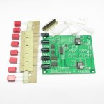
Attachments
Hi,
You could try a common base circuit like the one in this thread
In a common base stage the 'Input transistor' functions like current buffer and performs impedance matching only.
As it doesn't follow a exponential Working curve but simply performs current-in --> current-out its highly linear without relying on feedback .... and as such it s also very fast
It provides the DAC with the low impedance load it requires and looks like a high-impedance source for its own load, the I/V-resistor.
One can easily scale this resistor to generate the required signal voltage (+-1mA x R).
This Voltage can be used to drive either the following device or a output buffer stage (recommended).
Sonically such a simple discrete I/V stage can perform way better than any OPAmp equipped circuit I heard.
It puts music back into HiFi
jauu
Calvin
ps. I probabely cannot reply over the next two days
Hi,
You could try a common base circuit like the one in this thread
In a common base stage the 'Input transistor' functions like current buffer and performs impedance matching only.
As it doesn't follow a exponential Working curve but simply performs current-in --> current-out its highly linear without relying on feedback .... and as such it s also very fast
It provides the DAC with the low impedance load it requires and looks like a high-impedance source for its own load, the I/V-resistor.
One can easily scale this resistor to generate the required signal voltage (+-1mA x R).
This Voltage can be used to drive either the following device or a output buffer stage (recommended).
Sonically such a simple discrete I/V stage can perform way better than any OPAmp equipped circuit I heard.
It puts music back into HiFi
jauu
Calvin
ps. I probabely cannot reply over the next two days
Hi and thanks for answer...
I have been studing the thread; seems nice.
In post #7 of the thread http://www.diyaudio.com/forums/digital-source/266372-pcm1796-i-u-stage-cd-dac.html
Did anyone actually build that ?
Jesper.
Hi Jesper,
My conclusions from a small diy adventure perhaps could be helpful. When it comes to I/V conversion we have to consider signal level, DC offset and load presented at the DAC chip's output. The most common solution is to use a single resistor from current output to ground. Then feed a gain stage. That's exactly what fetishizator -and similar- is. The bigger the I/V resistor, the higher the signal level but there are limitations to this. The chips don't like to see high impedance. Bad for performance and maybe for longevity. I use a PCM 1792 chip which delivers 7,8 mA. With 82 ohm I/V it could move directly my super sensitive amps. But the sound was not good. Fetishizator was my entry build on this adventure. Easy to build and the designer is very helpful answering to queries. I also once found a variation by T. Loesch with different transistors somewhere in the internet. The Zen I/V is going further. It presents an ideal load to the chip to squeeze the juice out of it. I never test it though. I moved to tube gain stage after the I/V resistor. Very convinient as gain is usually high and grids do not care that much about the presence of a little - or a little more - DC offset. In my case, I ended up using 2 ohm resistor. The DAC likes this very much. And DC offset is down to 11 mV. Next move was to connect it directly to DCG3. It doesn't seem to care about this small DC offset. Sound is a dream. I have to tell that DCG3 is set to 6x gain and my amps also have more than enough gain. If you need higher output signal from the DAC, meaning raising the value of the resistor and consequently the DC offset, you could use coupling capacitors.
Another I/V conversion scheme is with transformers. See DDDAC. I never test this.
Kostas
Last edited:
Hi,
The ZEN is a symmetrical grounded-gate JFET circuit which is even better suited for the AD1856 but where the sourcing of parts may become critical and a suiting power supply may be not so easy (except for a battery supply).
I showed a bipolar Version of the ZEN rather early in that same thread, where the parts are easier to source.
Then there´s a very similar Nelson Pass I/V utilizing Mosfets.
Common to all these circuits is that the active devices simply pass the DAC current into external I/V resistors ... which means they only do impedance matching.
impedance matching or precise impedance mismatch is the key word when using a I/V resistor directly at the DAC output.
A current output DAC wants to see a as low as possible (ideally 0R) load.
They don´t like to see a higher impedance ... the more so the lower the DAC´s internal impedance is (only 1.7k for the AD1856).
Also the signal voltage dropping over the I/V resistor may trigger internal protection diodes ... which limits the output voltage to less than ~300mV before the diodes start conduction.
The direct I/V conversion thus requires a voltage gain stage to get the output voltage level to the desired value.
I don´t recommend that way of I/V conversion.
A active grounded-something stage feeding a I/V resistor and maybe a simple output buffer stage are giving the best results with least hassle.
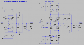
Attached are two symmetrical bipolar I/V stages.
The first beeing simpler, but due to the connection of the I/V resistors (Rivx) towards the supply lines with low PSRRR --> hence highquality supplies required
The second with current sources shielding against the supply lines and the Rivs connected to gnd (the bipolars can be sourced very cheap as matched Duals ... BC847/857, BC807/817 ... and even matched Quads ... THAT 300 series for example).
jauu
Calvin
Yes, I did .... and many more built such grounded-base or grounded-gate style circuits (see the JockoHomo or OPC´s MOSFET circuit for example)Did anyone actually build that ?
The ZEN is a symmetrical grounded-gate JFET circuit which is even better suited for the AD1856 but where the sourcing of parts may become critical and a suiting power supply may be not so easy (except for a battery supply).
I showed a bipolar Version of the ZEN rather early in that same thread, where the parts are easier to source.
Then there´s a very similar Nelson Pass I/V utilizing Mosfets.
Common to all these circuits is that the active devices simply pass the DAC current into external I/V resistors ... which means they only do impedance matching.
impedance matching or precise impedance mismatch is the key word when using a I/V resistor directly at the DAC output.
A current output DAC wants to see a as low as possible (ideally 0R) load.
They don´t like to see a higher impedance ... the more so the lower the DAC´s internal impedance is (only 1.7k for the AD1856).
Also the signal voltage dropping over the I/V resistor may trigger internal protection diodes ... which limits the output voltage to less than ~300mV before the diodes start conduction.
The direct I/V conversion thus requires a voltage gain stage to get the output voltage level to the desired value.
I don´t recommend that way of I/V conversion.
A active grounded-something stage feeding a I/V resistor and maybe a simple output buffer stage are giving the best results with least hassle.
Attached are two symmetrical bipolar I/V stages.
The first beeing simpler, but due to the connection of the I/V resistors (Rivx) towards the supply lines with low PSRRR --> hence highquality supplies required
The second with current sources shielding against the supply lines and the Rivs connected to gnd (the bipolars can be sourced very cheap as matched Duals ... BC847/857, BC807/817 ... and even matched Quads ... THAT 300 series for example).
jauu
Calvin
Attachments
Hi MagicBus, and welcome
So is this connection directly from the I/V resistor, or through a buffer?
There are a lot of things i cannot figure out yet regarding i/v conversion, but things come slowly to my mind now!
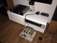
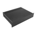
Anyway, i have ordred a chassis (yes ordred) for this DAC project, giving me space for all the psu's, and space for other dac in time.
So by some time i hope i can figure out howto create an i/v converter
Jesper.
...Next move was to connect it directly to DCG3. It doesn't seem to care about this small DC offset. Sound is a dream
So is this connection directly from the I/V resistor, or through a buffer?
There are a lot of things i cannot figure out yet regarding i/v conversion, but things come slowly to my mind now!
Anyway, i have ordred a chassis (yes ordred) for this DAC project, giving me space for all the psu's, and space for other dac in time.
So by some time i hope i can figure out howto create an i/v converter
Jesper.
Hi,
Yes, I did .... and many more built such grounded-base or grounded-gate style circuits (see the JockoHomo or OPC´s MOSFET circuit for example)
The ZEN is a symmetrical grounded-gate JFET circuit which is even better suited for the AD1856 but where the sourcing of parts may become critical and a suiting power supply may be not so easy (except for a battery supply).
I showed a bipolar Version of the ZEN rather early in that same thread, where the parts are easier to source.
Then there´s a very similar Nelson Pass I/V utilizing Mosfets.
Common to all these circuits is that the active devices simply pass the DAC current into external I/V resistors ... which means they only do impedance matching.
impedance matching or precise impedance mismatch is the key word when using a I/V resistor directly at the DAC output.
A current output DAC wants to see a as low as possible (ideally 0R) load.
They don´t like to see a higher impedance ... the more so the lower the DAC´s internal impedance is (only 1.7k for the AD1856).
Also the signal voltage dropping over the I/V resistor may trigger internal protection diodes ... which limits the output voltage to less than ~300mV before the diodes start conduction.
The direct I/V conversion thus requires a voltage gain stage to get the output voltage level to the desired value.
I don´t recommend that way of I/V conversion.
A active grounded-something stage feeding a I/V resistor and maybe a simple output buffer stage are giving the best results with least hassle.
Attached are two symmetrical bipolar I/V stages.
The first beeing simpler, but due to the connection of the I/V resistors (Rivx) towards the supply lines with low PSRRR --> hence highquality supplies required
The second with current sources shielding against the supply lines and the Rivs connected to gnd (the bipolars can be sourced very cheap as matched Duals ... BC847/857, BC807/817 ... and even matched Quads ... THAT 300 series for example).
jauu
Calvin
Hi Calvin...
I somewhat posted at the same time you did
Well you wrote
; do you meen the Nelson Pass Zen, or the Sen -> Cen -> Zen battery powered unit. -The ZEN is a symmetrical grounded-gate JFET circuit which is even better suited for the AD1856 but where the sourcing of parts may become critical and a suiting power supply may be not so easy (except for a battery supply).
I have a good part stock of 2sk170bl / 23j74bl / 2sk170gr, so if you meen that it could be a problem, it is not at moment.
I also read the Pass article, but i though that having enough voltage swing (preferbaly cd level ~2vrms), would not be easy with the AD1856's +-1mA current out???
Jesper.
No buffer, directly from I/V resistor. But... I use a dac with high current output so I managed to use a very small resistor to address all issues explained by Calvin. Your chip is different thus I think you should follow Calvin's suggestions. Just keep in mind that you allready have a great preampHi MagicBus, and welcome
...
So is this connection directly from the I/V resistor, or through a buffer?
...
Jesper.
that can be set for higher gain and it can't tolerate DC at its input.No buffer, directly from I/V resistor. But... I use a dac with high current output so I managed to use a very small resistor to address all issues explained by Calvin. Your chip is different thus I think you should follow Calvin's suggestions. Just keep in mind that you allready have a great preamp
Yes... i see, and i got it also i guess
...I also think Calvins solutions must be good, but i am not right capable of figuring enough out to build one myself, without any help.
I ofcause like the Pass design, as i know most of it works for me, but still i think it will deliver way to little voltage-swing for my DCG3 as for now. -Lets see how it goes... now i am just waiting for my chassis to arrive here in DK.
Jesper.
Attachments
Calvin...
Really appreciate youre writing/explanation here!
I read youre post some times, and included some googling along, for best understanding.
It really helped me understanding how it works, when you did write this :
So, Calvin if you where me, where would you start? -I also must say, that i am having +12 / -12 (SSLV1.1 homerolled) and +5 and +3.3 ReflectorD (also homerolled) Ofcause i can make another psu for any i/v converter, but if it's possible to use the one, which is allready made for the DAC, it would be pleasant.
Jesper.
Really appreciate youre writing/explanation here!
I read youre post some times, and included some googling along, for best understanding.
It really helped me understanding how it works, when you did write this :
Making me understand, that most important is that DAC sees lowish impedance (near "0") for making it behave best.Common to all these circuits is that the active devices simply pass the DAC current into external I/V resistors ... which means they only do impedance matching.
impedance matching or precise impedance mismatch is the key word when using a I/V resistor directly at the DAC output.
So, Calvin if you where me, where would you start? -I also must say, that i am having +12 / -12 (SSLV1.1 homerolled) and +5 and +3.3 ReflectorD (also homerolled) Ofcause i can make another psu for any i/v converter, but if it's possible to use the one, which is allready made for the DAC, it would be pleasant.
Jesper.
As always it is all about compromise. You choose your poison...
What are your priorities?
For me a coupling cap in this particular spot is simply unjustified, both as a source of colouration and as an expense, as the reasonably good ones cost real money.
Faced with the coupling cap dilemma even opamps begin to look good.
If severe levels of nfb are undesirable, then passive conversion + tube gain stage looks very attractive. For some obscure reason most of these implementations waste a transformer after the conversion resistor and cap-couple the tube output.
And then, there are the no nfb chip solutions around AD844 and similar ICs. In some cases these can work without coupling caps, which makes them very attractive in my eyes.
As always it is all about compromise. You choose your poison...
What are your priorities?
Not really having some priority here for now!
If you have read the first post, where i tell about how this dac sounds :
there was no doubt that this new dac is smoother and less sibiliance-aggresive.
I am just in the spirit of my diy chasing the even better sound
Thanks for youre input!
Jesper.
Hi,
I thought of EUVL's SEN-ZEN, but NP's ZEN is basically the same in MOSFET.
EUVL's circuit is a bit special in that it requires a floating supply, which iIrc was a source of trouble for some users.
The other suggested circuits all use symmetrical gnd-referenced supplies.
I don't share the negative about coupling caps and seriously doubt the often reported 'differences' in sound.
When evaluated under just slightly serious test conditions the huge differences typically crumble to tiny pieces.
Also, the measurements required to get rid of the cap are more complex, more non-linear (trafos) or require even more caps (dc servo).
It seems to me that the simple circuits often have a certain sonic charme, a naturalness and musicality that more complex circuits begin loose.
The afore mentioned AD844 (and the imho preferrable and cheaper OPA860 and OPA861) could beak that rule.
All three ICs base on the symmetrical grounded base topology, similar to the second circuit in #6.
They replace the current sources Q3a/q4a and the double Riv/Civ by current mirrors.
The input leg transistors of the CMs are found at Q3a/Q4a positions and the collectors of the output legs are tied together (node TZ from AD844).
From this node one Riv/Civ is connected to gnd.
So the current mirrors replace the current sources plus the dc blocking caps C1/C2.
Same as the current source equipped circuit, the current mirrors shield against power supply, hence the PSRR is high.
This topology can easily be implemented using discrete matched Duals, running them on sufficiently high idle current.
Between the TZ node and its output the AD844 features a bipolar diamond buffer and as usual with ICs, under the hood there are additional helper circuits and typically more complex strucures.
Some users circumvented the low idle current problem by paralleling two or more of the ADs.
The OPAs are almost identical (one features a diamond buffer too, the other comes wo a buffer stage).
The major differences are higher idle current but lower supply voltage range (+-5V).
One OPA can replace almost two ADs (gaining even more on cost)
As long as the max, output voltage remains well within the voltage limits (~4V iIrc) a higher idle current is advantageous.
The voltage calculates to V= Idac x Riv.
Example: Idac = +-1mApp = 0.7mArms
If Riv = 3kOhm, then V = +-3Vpp = 2.1Vrms
The OPAs are good for almost 3Vrms.
As the maximum DAC current is defined and fix one doesn't need to design the I/V stage with voltage overhead in mind.
Under no circumstances can V exceed the I x R value (unlike for example a phono stage, where clicks and pops can easily exceed the input signal and drive the circuit into overload/clipping).
The ICs are certainly the easiest way to implement a sonically top notch I/V converter stage utilizing the open loop grounded base topology.
jauu
Calvin
The I/V resistor is the "virtual short" seen by the current source (DAC) when it is connected directly to the inverting input of the op-amp. So the op-amp does all the work - you don't need a separate I/V resistor.
What I don't really like about these op-amps is that this "virtual short" is not really a short. For example, the AD844 appears like a ~50R resistor. The OPA860/1 seem to be better (at ~13R if I'm reading the datasheet correctly).
I may be wrong of course, I'm just now trying to go a little deeper on I/V converters due to an ES9038 that I'm thinking about building.
Hi,
Yes and No.
Yes, as the Riv doesn´t affect the DAC´s performance anymore and ...
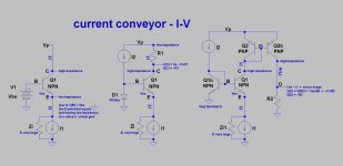
No, as the circuit doesn´t amplify the current but rather ´conveys´ it to its output (these circuits are hence named ´current conveyors´).
While some of the simplest circuits really convey do the more complex ones rather create an precise image of the DAC current ....
and Yes again, as circuits using the current mirrors like the AD and the OPAs could be designed to scale that image current, hence amplify.
In discrete form one could for example change the resistors in the output legs of the mirrors, or simply double/triple the complete output legs.
See the thrid circuit of the attachment.
All three show just the ´positive´ branch of the whole.
The AD844 and the OPA86x are just doubled (complementars) and the output of the second current mirror would be connected to node ´D´ and R2 forms the I/V resistor.
In all three circuits node ´E´ is a low impedance input for the DAC-current.
The idle dc-currents I1 and the DAC´s signal currents add up and appear at the nodes ´C´.
´C´ are high-impedance collector outputs.
As such nodes ´C´ are good curent sources.
R1 in the middle circuit forms the Riv.
R1 beeing connected to the power supply, the node ´C´ has a dc-offset voltage, so that a DC-blocking cap is needed to couple the signal to the output ( for maximum possible volatge swing I1 is chosen so that V(c) settles at ~Vp/2).
Also every disturbance on the supply line couples through R1 into the output.
In the third circuit the curent appearing at node ´C´ flows through Q2 the input leg of the current mirror Q2/Q2b.
A precise image of the current appears at the collector of Q2b, node ´D´.
Doubling or mulriplying Q2b doubles or multiplies the current into node ´D´.
That doubles or multiplies the voltage over R2.
On the opposite, for same voltage R2 could be halved or divided in value.
If You don´t amplify but rather copy the input signal, the circuit is typically called a Buffer.
A voltage buffer stage copies (or better transfers or conveys) the input voltage to its output matches the impedances, the current conveyor or current buffer does the same but copies (transfers, or conveys) input current to its output and matches impedances.
The difference is in the impedances values.
While the voltage buffer presents the source device a high impedance and its load device a low impedance, the current buffer does the opposite ... low input impedance and high output impedance.
The impedance matching is required as all the AudioDACs span a rather medium output impedance ranging between a couple of hundred Ohms to ~3kOhm.
So they are rather a mixture between a low-impedance voltage source and a high-impedance current source.
In other words are they only mediocre quality current sources.
The second reason is the low voltage compliance of their outputs.
Voltage compliance is typically not specced, but as a rule of thumb its less than +-1V and quite often not even symmetrical.
The voltage compliance at the output of the current buffers can be much higher ... so high in fact that the output signal voltage is sufficient to drive a loudspeaker if a accordingly powerful (voltage) buffer stage is added -> Power DAC.
The I/V converter would then take over the role of the input and VAS-stage in a power amplifier.
jauu
Calvin
ps. DimDims remarks about the not really low input impedance of especially the single AD844 is correct.
With a simple discrete input transistor You can achieve lower input impedance values down to ~1R.
With CFP connected transistors You can achieve impedance values down to a few mOhms.
Plus, You can choose the idle currents considerably higher and Your not bound to the typical power supply voltage limits of OPAmps
Yes and No.
Yes, as the Riv doesn´t affect the DAC´s performance anymore and ...
No, as the circuit doesn´t amplify the current but rather ´conveys´ it to its output (these circuits are hence named ´current conveyors´).
While some of the simplest circuits really convey do the more complex ones rather create an precise image of the DAC current ....
and Yes again, as circuits using the current mirrors like the AD and the OPAs could be designed to scale that image current, hence amplify.
In discrete form one could for example change the resistors in the output legs of the mirrors, or simply double/triple the complete output legs.
See the thrid circuit of the attachment.
All three show just the ´positive´ branch of the whole.
The AD844 and the OPA86x are just doubled (complementars) and the output of the second current mirror would be connected to node ´D´ and R2 forms the I/V resistor.
In all three circuits node ´E´ is a low impedance input for the DAC-current.
The idle dc-currents I1 and the DAC´s signal currents add up and appear at the nodes ´C´.
´C´ are high-impedance collector outputs.
As such nodes ´C´ are good curent sources.
R1 in the middle circuit forms the Riv.
R1 beeing connected to the power supply, the node ´C´ has a dc-offset voltage, so that a DC-blocking cap is needed to couple the signal to the output ( for maximum possible volatge swing I1 is chosen so that V(c) settles at ~Vp/2).
Also every disturbance on the supply line couples through R1 into the output.
In the third circuit the curent appearing at node ´C´ flows through Q2 the input leg of the current mirror Q2/Q2b.
A precise image of the current appears at the collector of Q2b, node ´D´.
Doubling or mulriplying Q2b doubles or multiplies the current into node ´D´.
That doubles or multiplies the voltage over R2.
On the opposite, for same voltage R2 could be halved or divided in value.
If You don´t amplify but rather copy the input signal, the circuit is typically called a Buffer.
A voltage buffer stage copies (or better transfers or conveys) the input voltage to its output matches the impedances, the current conveyor or current buffer does the same but copies (transfers, or conveys) input current to its output and matches impedances.
The difference is in the impedances values.
While the voltage buffer presents the source device a high impedance and its load device a low impedance, the current buffer does the opposite ... low input impedance and high output impedance.
The impedance matching is required as all the AudioDACs span a rather medium output impedance ranging between a couple of hundred Ohms to ~3kOhm.
So they are rather a mixture between a low-impedance voltage source and a high-impedance current source.
In other words are they only mediocre quality current sources.
The second reason is the low voltage compliance of their outputs.
Voltage compliance is typically not specced, but as a rule of thumb its less than +-1V and quite often not even symmetrical.
The voltage compliance at the output of the current buffers can be much higher ... so high in fact that the output signal voltage is sufficient to drive a loudspeaker if a accordingly powerful (voltage) buffer stage is added -> Power DAC.
The I/V converter would then take over the role of the input and VAS-stage in a power amplifier.
jauu
Calvin
ps. DimDims remarks about the not really low input impedance of especially the single AD844 is correct.
With a simple discrete input transistor You can achieve lower input impedance values down to ~1R.
With CFP connected transistors You can achieve impedance values down to a few mOhms.
Plus, You can choose the idle currents considerably higher and Your not bound to the typical power supply voltage limits of OPAmps
Attachments
Last edited:
Opamp's
Hi... I am listening here
Nice to see all the post; anyway i have no problem trying opamp's, as long they are considered "good" quality parts.
It would also be fun to then compare the Iout from the DAC to the Vout. (Easy to do A/B here)
I see, that OPA860's only come in "smd" part; i never tried solder that stuff, but i think it would be doable creating some sort of smd to through-hole socket!
IF? I choose to try, say the OPA860, can some of you perhaps post a schematic to start with?
Regards; Jesper.
OPA smd. ::
Attachments
Thank you very much for your reply Calvin! I'll have to read it many times but I allready understand things better. One thing I would like to clarify for starters;
Does this mean that the dac depends on optimal load to swing its maximum output current? What if the dac's build in volume control is been used to reduce output level - and disregard the digital headroom loss? Could the dac then tolerate a little higher load impedance? Perhaps my question is meaningless though....
In other words are they only mediocre quality current sources.
The second reason is the low voltage compliance of their outputs.
...
I hope I'm working for both of usHi... I am listening here
...
- Status
- This old topic is closed. If you want to reopen this topic, contact a moderator using the "Report Post" button.
- Home
- Source & Line
- Digital Line Level
- AD1856 I/V (I/U) converter