Wayne turned me on to some parts for this, and I have
started re-working the pc board to fit the sinks in the store.
")
TIP142 and TIP147 are $2-ish each at Digikey. It wold cool to have extra output devices in parallel to be able to drive 200W into 4 ohms, 400watts into 2 ohms and 800 watts into 1 ohms with the proper number of output devices.
It would also be cool to be able to run the entire amp at class A up to 20 watts if desired.
With the output devices operated as followers, and 1 ohm emitter resistors, how important would it be to match output devices for Vce and/or current gain? Or, if the output devices are highly matched, can the emitter resistors be reduced or eliminated?
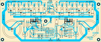
Just try to "help" PCB layout
This is a layout from my "perspective".
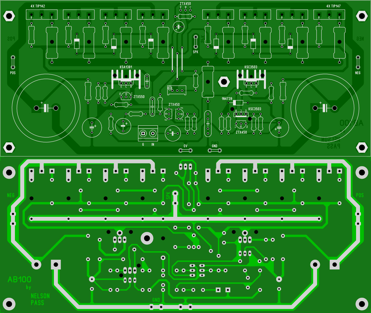
190*80mm
I think maybe ZTX450/550 could be changed to 2N5551/5401 (pin-to-pin compatible)
Q3 might be quite hot (somewhere about 200mW for ±50V supply). BC639 might also works as good.
2mm holes are just to help ventilation / cooling the devices around it, so it should be more reliable I guess.
edit : R8 best be ½~1Watt resistor. You may want to change the layout a bit.
ZIP :
*.Lay6 files (Sprint-Layout 6)
Gerber Files & Drill
feel free to modify it if you find some missing track, too long track, or want to change parts layout
I'm not about to build this amp though. I already satisfied with my class-AB LME49811.
This is a layout from my "perspective".
190*80mm
I think maybe ZTX450/550 could be changed to 2N5551/5401 (pin-to-pin compatible)
Q3 might be quite hot (somewhere about 200mW for ±50V supply). BC639 might also works as good.
2mm holes are just to help ventilation / cooling the devices around it, so it should be more reliable I guess.
edit : R8 best be ½~1Watt resistor. You may want to change the layout a bit.
ZIP :
*.Lay6 files (Sprint-Layout 6)
Gerber Files & Drill
feel free to modify it if you find some missing track, too long track, or want to change parts layout
I'm not about to build this amp though. I already satisfied with my class-AB LME49811
.Attachments
Last edited:
Can't edit posts after 30 minutes.
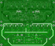
Just realize that I've put too many jumper
you might want to swap the position of speaker terminal (lug?) with the trimpot (& R15) and relayout a bit, thus eliminating all jumper.
5 AM & still awake!
Just realize that I've put too many jumper
you might want to swap the position of speaker terminal (lug?) with the trimpot (& R15) and relayout a bit, thus eliminating all jumper.
5 AM & still awake!
Attachments
Last edited:
Kroto
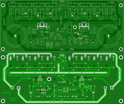
Excellent layout. I would agree swapping the trimpot with the speaker lug. It would eliminate the long trace to the trimpot. ...or, just use jumpers or a top layer to eliminate any long traces. Double sided boards cannot be much more costly than single sided boards.
I have a small stash of KSA/KSC parts for the drivers.
It would be interesting to have a board for paralleling many more output devices similar to how some of the Diyaudio Store amplifiers have separate driver and output boards.
Maybe like this? :Kroto
Excellent layout. I would agree swapping the trimpot with the speaker lug. It would eliminate the long trace to the trimpot. ...or, just use jumpers or a top layer to eliminate any long traces. Double sided boards cannot be much more costly than single sided boards.
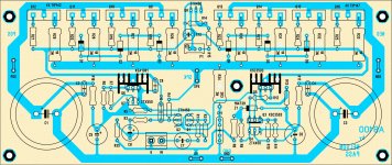
Actually, those KSC/KSA (/w heatsink) are not drivers, they were CCS and VAS. The drivers is inside TIP14x.I have a small stash of KSA/KSC parts for the drivers.
I'm not sure why the schematic use enormously big bypass capacitor (2x 10mF/rail (C1-C4)).
To fit the PCB nicely I put only one big lytics/rail (C1, C3) and the other cap is film type (C2, C4).
The input cap is so big, that it might be hard to fit any film cap, so I put electrolytic type, maybe SILMIC II ok.
The original schematic use no Miller cap (C9), I'm not sure wheter this layout will safe from osc' with too long traces.It would be interesting to have a board for paralleling many more output devices similar to how some of the Diyaudio Store amplifiers have separate driver and output boards.
Attachments
Maybe like this? :
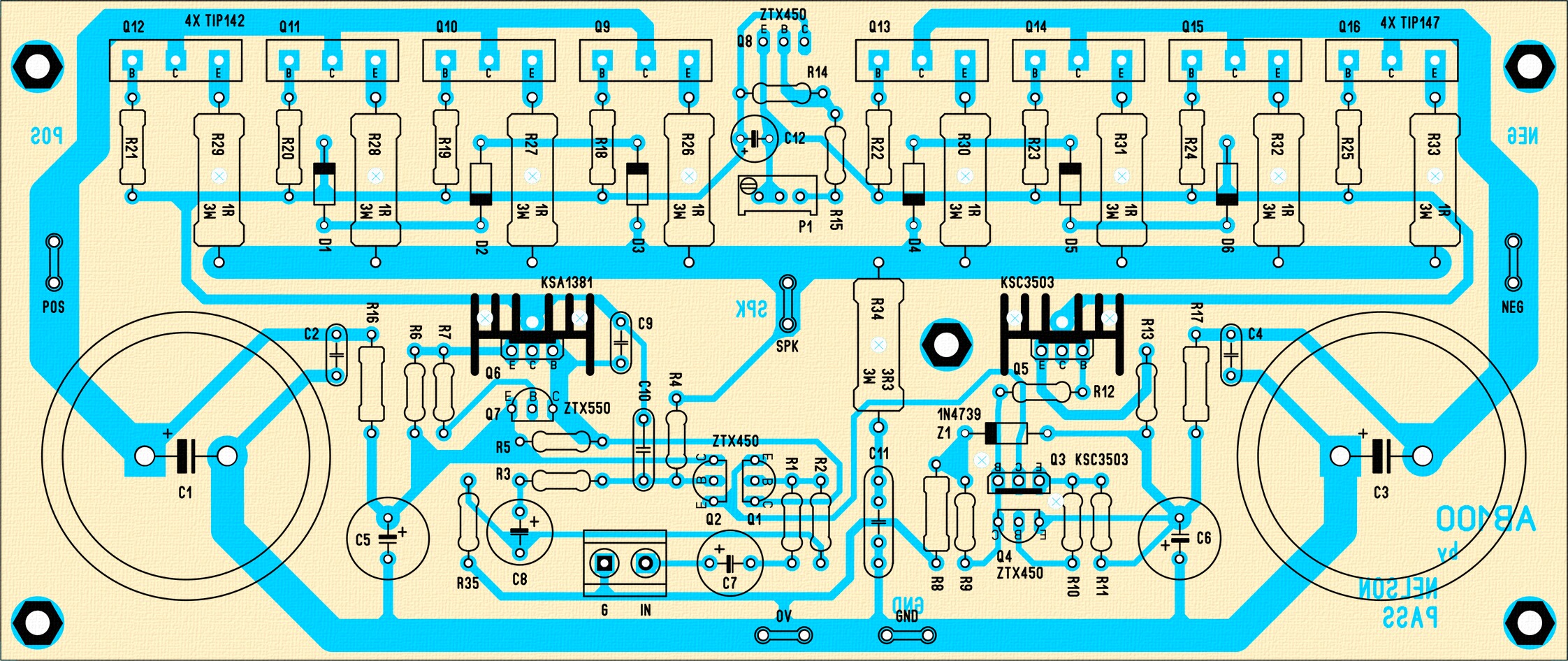
Actually, those KSC/KSA (/w heatsink) are not drivers, they were CCS and VAS. The drivers is inside TIP14x.
I'm not sure why the schematic use enormously big bypass capacitor (2x 10mF/rail (C1-C4)).
To fit the PCB nicely I put only one big lytics/rail (C1, C3) and the other cap is film type (C2, C4).
The input cap is so big, that it might be hard to fit any film cap, so I put electrolytic type, maybe SILMIC II ok.
The original schematic use no Miller cap (C9), I'm not sure wheter this layout will safe from osc' with too long traces.
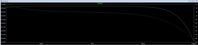
Hi, nice PCB,
I think they are (c1-c4) not bay pass capacitors - but the main filter capacitors. Input cap also can be reduced - i used 2.2uf .
Maybe you can add some film bypass cap across feedback capacitor.
i attached sim of my ab100 with 2,2uf input an 100uf feedback cap
Attachments
Last edited:
Maybe like this? :
Actually, those KSC/KSA (/w heatsink) are not drivers, they were CCS and VAS. The drivers is inside TIP14x.
I'm not sure why the schematic use enormously big bypass capacitor (2x 10mF/rail (C1-C4)).
To fit the PCB nicely I put only one big lytics/rail (C1, C3) and the other cap is film type (C2, C4).
The input cap is so big, that it might be hard to fit any film cap, so I put electrolytic type, maybe SILMIC II ok.
The original schematic use no Miller cap (C9), I'm not sure wheter this layout will safe from osc' with too long traces.
Can you post the updated board files? This is a very nice layout. The routes are short and the parts are well-placed.
By driver, I meant VAS. I bought some of these KSA/KSC parts for the VAS of the VSSA CFB amp but never used them.
Hi, nice PCB,
I think they are (c1-c4) not bay pass capacitors - but the main filter capacitors. Input cap also can be reduced - i used 2.2uf .
Maybe you can add some film bypass cap across feedback capacitor.
i attached sim of my ab100 with 2,2uf input an 100uf feedback cap
Can you post your .asc?
here's the file: (I use MJE15030 / 31 and ztx450 / 550 and MJ darlingtons in a real amplifier)
transistor models:
.model MJE15030 NPN(IS=3.894e-11 BF=312.524 NF=1.0979 VAF=9.9963 IKF=0.796201 ISE=2.37397e-09 NE=1.94897 BR=0.14246 NR=1.64791 VAR=99.9749 IKR=0.00539895 ISC=2.33175e-09 NC=2.79024 RB=267.202 IRB=9.99994e-13 RBM=0.299835 RE=3.04316e-05 RC=0.252928 XTB=0.1 XTI=3.92812 EG=1.05 CJE=2.42998e-09 VJE=0.794171 MJE=0.569313 TF=1.87986e-09 XTF=1000 VTF=1835.34 ITF=270.188 CJC=2.43127e-10 VJC=0.4 MJC=0.361453 XCJC=0.802892 FC=0.8 CJS=0 VJS=0.75 MJS=0.5 TR=9.86194e-06 PTF=0 KF=0 AF=1)
.model MJE15031 PNP(IS=7.17489e-11 BF=457.169 NF=1.11376 VAF=6.01557 IKF=0.345808 ISE=1e-08 NE=2.18567 BR=0.247882 NR=1.39549 VAR=60.1557 IKR=0.0263893 ISC=1e-16 NC=2.89486 RB=2.29208 IRB=0.0
.MODEL ZTX450 NPN IS =3.941445E-14 BF =175 VAF=109.45 NF =1 IKF=.8
+ISE=7.4025E-15 NE =1.3 BR =20.5 VAR=14.25 NR =.974 IKR=.1 ISC=3.157E-13
+NC =1.2 RB =1.1 RE =.1259 RC =.0539 CJE=63E-12 TF =.75E-9 CJC=15.8E-12
+TR =85E-9 VJC=.505 MJC=.39
.MODEL BD135_137_139 NPN ( IS=2.3985E-13 BF=244.9 NF=1.0 BR=78.11 NR=1.007 ISE=1.0471E-14 NE=1.2 ISC=1.9314E-11 NC=1.45 VAF=98.5 VAR=7.46 IKF=1.1863 IKR=0.1445 RB=2.14 RBM=0.001 IRB=0.031 RE=0.0832 RC=0.01 CJE=2.92702E-10 VJE=0.67412 MJE=0.3300 FC=0.5 CJC=4.8831E-11 VJC=0.5258 MJC=0.3928 XCJC=0.5287 XTB=1.1398 EG=1.2105 XTI=3.0)
.MODEL BD136_138_140 PNP ( IS=2.9537E-13 BF=201.4 NF=1.0 BR=23.765 NR=1.021 ISE=1.8002E-13 NE=1.5 ISC=7.0433E-12 NC=1.38 VAF=137.0 VAR=8.41 IKF=1.0993 IKR=0.10 RB=1.98 RBM=0.01 IRB=0.011 RE=0
.model MPS8099 NPN(Is=4.872f Xti=3 Eg=1.11 Vaf=100 Bf=9.599K Ne=1.315 Ise=14.65f Ikf=.1434 Xtb=1.5 Br=6.935 Nc=2 Isc=0 Ikr=0 Rc=.7 Cjc=5.805p Mjc=.4312 Vjc=.75 Fc=.5 Cje=10.49p Mje=.4602 Vje=.75 Tr=565p Tf=407p Itf=.18 Vtf=3 Xtf=2.5 Rb=10)
.model MPS8599 PNP(Is=10.68f Xti=3 Eg=1.11 Vaf=100 Bf=187.7 Ne=1.401 Ise=26.07f Ikf=.2203 Xtb=1.5 Br=1.833 Nc=2 Isc=0 Ikr=0 Rc=.8 Cjc=14.16p Mjc=.5585 Vjc=.75 Fc=.5 Cje=25.11p Mje=.3626 Vje=.
Attachments
here's the file: (I use MJE15030 / 31 and ztx450 / 550 and MJ darlingtons in a real amplifier)
transistor models:
.model MJE15030 NPN(IS=3.894e-11 BF=312.524 NF=1.0979 VAF=9.9963 IKF=0.796201 ISE=2.37397e-09 NE=1.94897 BR=0.14246 NR=1.64791 VAR=99.9749 IKR=0.00539895 ISC=2.33175e-09 NC=2.79024 RB=267.202 IRB=9.99994e-13 RBM=0.299835 RE=3.04316e-05 RC=0.252928 XTB=0.1 XTI=3.92812 EG=1.05 CJE=2.42998e-09 VJE=0.794171 MJE=0.569313 TF=1.87986e-09 XTF=1000 VTF=1835.34 ITF=270.188 CJC=2.43127e-10 VJC=0.4 MJC=0.361453 XCJC=0.802892 FC=0.8 CJS=0 VJS=0.75 MJS=0.5 TR=9.86194e-06 PTF=0 KF=0 AF=1)
.model MJE15031 PNP(IS=7.17489e-11 BF=457.169 NF=1.11376 VAF=6.01557 IKF=0.345808 ISE=1e-08 NE=2.18567 BR=0.247882 NR=1.39549 VAR=60.1557 IKR=0.0263893 ISC=1e-16 NC=2.89486 RB=2.29208 IRB=0.0
.MODEL ZTX450 NPN IS =3.941445E-14 BF =175 VAF=109.45 NF =1 IKF=.8
+ISE=7.4025E-15 NE =1.3 BR =20.5 VAR=14.25 NR =.974 IKR=.1 ISC=3.157E-13
+NC =1.2 RB =1.1 RE =.1259 RC =.0539 CJE=63E-12 TF =.75E-9 CJC=15.8E-12
+TR =85E-9 VJC=.505 MJC=.39
.MODEL BD135_137_139 NPN ( IS=2.3985E-13 BF=244.9 NF=1.0 BR=78.11 NR=1.007 ISE=1.0471E-14 NE=1.2 ISC=1.9314E-11 NC=1.45 VAF=98.5 VAR=7.46 IKF=1.1863 IKR=0.1445 RB=2.14 RBM=0.001 IRB=0.031 RE=0.0832 RC=0.01 CJE=2.92702E-10 VJE=0.67412 MJE=0.3300 FC=0.5 CJC=4.8831E-11 VJC=0.5258 MJC=0.3928 XCJC=0.5287 XTB=1.1398 EG=1.2105 XTI=3.0)
.MODEL BD136_138_140 PNP ( IS=2.9537E-13 BF=201.4 NF=1.0 BR=23.765 NR=1.021 ISE=1.8002E-13 NE=1.5 ISC=7.0433E-12 NC=1.38 VAF=137.0 VAR=8.41 IKF=1.0993 IKR=0.10 RB=1.98 RBM=0.01 IRB=0.011 RE=0
.model MPS8099 NPN(Is=4.872f Xti=3 Eg=1.11 Vaf=100 Bf=9.599K Ne=1.315 Ise=14.65f Ikf=.1434 Xtb=1.5 Br=6.935 Nc=2 Isc=0 Ikr=0 Rc=.7 Cjc=5.805p Mjc=.4312 Vjc=.75 Fc=.5 Cje=10.49p Mje=.4602 Vje=.75 Tr=565p Tf=407p Itf=.18 Vtf=3 Xtf=2.5 Rb=10)
.model MPS8599 PNP(Is=10.68f Xti=3 Eg=1.11 Vaf=100 Bf=187.7 Ne=1.401 Ise=26.07f Ikf=.2203 Xtb=1.5 Br=1.833 Nc=2 Isc=0 Ikr=0 Rc=.8 Cjc=14.16p Mjc=.5585 Vjc=.75 Fc=.5 Cje=25.11p Mje=.3626 Vje=.
Got it. Thanks. The symbols for the output transistors are missing. Can you post them?
I use : mj11016/15
.SUBCKT mj11015 1 2 3
* Model generated on Feb 14, 2004
* Model format: PSpice
* Darlington macro model
* External node designations
* Node 1 -> Collect
* Node 2 -> Base
* Node 3 -> Emitter
Q1 1 2 4 qmodel
Q2 1 4 3 q1model 19.7144
D1 1 3 dmodel
R1 2 4 8000
R2 4 3 40
* Default values used in dmodel
* EG=1.11 TT=0 BV=infinite
.MODEL dmodel d
+IS=1e-12 RS=10.3385 N=1.00339 XTI=3.00339
+CJO=0 VJ=0.75 M=0.33 FC=0.5
.MODEL qmodel pnp
+IS=6.3079e-13 BF=209.535 NF=0.85 VAF=179.833
+IKF=0.221129 ISE=4.68834e-12 NE=1.25754 BR=0.969262
+NR=0.75 VAR=138.099 IKR=0.0995603 ISC=1e-13
+NC=2.00339 RB=7.45687 IRB=0.203385 RBM=7.45687
+RE=0.107979 RC=1.34582 XTB=0.486317 XTI=3.00541 EG=1.19211
+CJE=1e-11 VJE=0.75 MJE=0.33 TF=1e-09
+XTF=1 VTF=10 ITF=0.01 CJC=1e-11
+VJC=0.75 MJC=0.33 XCJC=0.9 FC=0.5
+TR=1e-07 PTF=0 KF=0 AF=1
.MODEL q1model pnp
+IS=6.3079e-13 BF=209.535 NF=0.85 VAF=179.833
+IKF=0.221129 ISE=4.68834e-12 NE=1.25754 BR=0.969262
+NR=0.75 VAR=138.099 IKR=0.0995603 ISC=1e-13
+NC=2.00339 RB=7.45687 IRB=0.203385 RBM=7.45687
+RE=0.107979 RC=1.34582 XTB=0.486317 XTI=3.00541 EG=1.19211
+CJE=1e-11 VJE=0.75 MJE=0.33 TF=1e-09
+XTF=1 VTF=10 ITF=0.01 CJC=0
+VJC=0.75 MJC=0.33 XCJC=0.9 FC=0.5
+TR=1e-07 PTF=0 KF=0 AF=1
.ENDS
.SUBCKT mj11016g 1 2 3
* Model generated on Apr 11, 11
* MODEL FORMAT: PSpice
* Darlington macro model
* External node designations
* Node 1 -> Collect
* Node 2 -> Base
* Node 3 -> Emitter
Q1 1 2 4 qmodel
Q2 1 4 3 q1model 29.3683
D1 3 1 dmodel
R1 2 4 8000
R2 4 3 40
* Default values used in dmodel
* EG=1.11 TT=0 BV=infinite
.MODEL dmodel d
+IS=1e-12 RS=0 N=0.863519 XTI=2.86352
+CJO=0 VJ=0.75 M=0.33 FC=0.5
.MODEL qmodel npn
+IS=7.46007e-16 BF=232.735 NF=0.85 VAF=30
+IKF=0.291159 ISE=7.00919e-11 NE=1.84137 BR=1.40703
+NR=0.751634 VAR=10.0112 IKR=0.101463 ISC=1e-13
+NC=1.86352 RB=3.12784 IRB=0.1 RBM=3.12784
+RE=0.351702 RC=1.75894 XTB=0.188551 XTI=2.86314 EG=1.05008
+CJE=1.904e-08 VJE=0.95 MJE=0.23 TF=1e-09
+XTF=1 VTF=10 ITF=0.01 CJC=3.24694e-10
+VJC=0.95 MJC=0.23 XCJC=0.9 FC=0.5
+TR=1e-07 PTF=0 KF=0 AF=1
.MODEL q1model npn
+IS=7.46007e-16 BF=232.735 NF=0.85 VAF=30
+IKF=0.291159 ISE=7.00919e-11 NE=1.84137 BR=1.40703
+NR=0.751634 VAR=10.0112 IKR=0.101463 ISC=1e-13
+NC=1.86352 RB=3.12784 IRB=0.1 RBM=3.12784
+RE=0.351702 RC=1.75894 XTB=0.188551 XTI=2.86314 EG=1.05008
+CJE=1.904e-08 VJE=0.95 MJE=0.23 TF=1e-09
+XTF=1 VTF=10 ITF=0.01 CJC=0
+VJC=0.95 MJC=0.23 XCJC=0.9 FC=0.5
+TR=1e-07 PTF=0 KF=0 AF=1
.ENDS
but i have also tip SUBCKT
.SUBCKT tip147 1 2 3
* Model generated on 14 Dec 2009
* Model format: LTspice
* Darlington macro model
* External node designations
* Node 1 -> Collector
* Node 2 -> Base
* Node 3 -> Emitter
Q1 1 2 4 qmodel
Q2 1 4 3 q1model 9.26065
D1 1 3 dmodel
R1 4 2 5000
R2 3 4 150
.MODEL dmodel d
+IS=1e-12 RS=10 N=1 XTI=3
+CJO=0 VJ=0.75 M=0.33 FC=0.5
.MODEL qmodel pnp
+IS=1.03024e-14 BF=50 NF=1.2 VAF=679.126
+IKF=0.190032 ISE=1.23159e-13 NE=1.73997 BR=1.10206
+NR=1.19838 VAR=126.182 IKR=0.103332 ISC=1.23159e-13
+NC=2 RB=5.06065 IRB=0.2 RBM=5.06065
+RE=0.199903 RC=2.01466 XTB=0.354371 XTI=3.01199 EG=1.206
+CJE=1e-11 VJE=0.75 MJE=0.33 TF=1e-09
+XTF=1 VTF=10 ITF=0.01 CJC=1.67157e-09
+VJC=0.95 MJC=0.23 XCJC=0.9 FC=0.5
+TR=1e-07 PTF=0 KF=0 AF=1
.MODEL q1model pnp
+IS=1.03024e-14 BF=60 NF=1.2 VAF=679.126
+IKF=0.190032 ISE=1.23159e-13 NE=1.73997 BR=1.10206
+NR=1.19838 VAR=126.182 IKR=0.103332 ISC=1.23159e-13
+NC=2 RB=5.06065 IRB=0.2 RBM=5.06065
+RE=0.199903 RC=2.01466 XTB=0.354371 XTI=3.01199 EG=1.206
+CJE=1e-11 VJE=0.75 MJE=0.33 TF=1e-09
+XTF=1 VTF=10 ITF=0.01 CJC=0
+VJC=0.95 MJC=0.23 XCJC=0.9 FC=0.5
+TR=1e-07 PTF=0 KF=0 AF=1
.ENDS
.SUBCKT tip142 1 2 3
* Model generated on 14 Dec 2009
* Model format: LTspice
* Darlington macro model
* External node designations
* Node 1 -> Collector
* Node 2 -> Base
* Node 3 -> Emitter
Q1 1 2 4 qmodel
Q2 1 4 3 q1model 9.26065
D1 3 1 dmodel
R1 4 2 5000
R2 3 4 150
.MODEL dmodel d
+IS=1e-12 RS=10 N=1 XTI=3
+CJO=0 VJ=0.75 M=0.33 FC=0.5
.MODEL qmodel npn
+IS=1.03024e-14 BF=50 NF=1.2 VAF=679.126
+IKF=0.190032 ISE=1.23159e-13 NE=1.73997 BR=1.10206
+NR=1.19838 VAR=126.182 IKR=0.103332 ISC=1.23159e-13
+NC=2 RB=5.06065 IRB=0.2 RBM=5.06065
+RE=0.199903 RC=2.01466 XTB=0.354371 XTI=3.01199 EG=1.206
+CJE=1e-11 VJE=0.75 MJE=0.33 TF=1e-09
+XTF=1 VTF=10 ITF=0.01 CJC=1.67157e-09
+VJC=0.95 MJC=0.23 XCJC=0.9 FC=0.5
+TR=1e-07 PTF=0 KF=0 AF=1
.MODEL q1model npn
+IS=1.03024e-14 BF=60 NF=1.2 VAF=679.126
+IKF=0.190032 ISE=1.23159e-13 NE=1.73997 BR=1.10206
+NR=1.19838 VAR=126.182 IKR=0.103332 ISC=1.23159e-13
+NC=2 RB=5.06065 IRB=0.2 RBM=5.06065
+RE=0.199903 RC=2.01466 XTB=0.354371 XTI=3.01199 EG=1.206
+CJE=1e-11 VJE=0.75 MJE=0.33 TF=1e-09
+XTF=1 VTF=10 ITF=0.01 CJC=0
+VJC=0.95 MJC=0.23 XCJC=0.9 FC=0.5
+TR=1e-07 PTF=0 KF=0 AF=1
.ENDS
I am slogging my way through trying get .asc to run. The missing symbols are *.asy files. I have downloaded one but it requires massaging. If you could load all of the not-portable stuff on the schematic, it would be appreciated.
I am looking to probe bias currents to create tests to match transistors. When it comes time to build, I want to be able to match pairs or quads. Possibly to reduce the emitter resistors and get more current output into low impedance loads.
I am looking to probe bias currents to create tests to match transistors. When it comes time to build, I want to be able to match pairs or quads. Possibly to reduce the emitter resistors and get more current output into low impedance loads.
I'm unfortunately not so good user of LTspice..
You should unzip and add attached files in the lib/sym folder under "darlingtons"
LTSPICE neophyte here as well. I posted a request for help on the LTSPICE thread.
yea, but Mr. Pass also use two really big electrolytics in B1 bufferI think they are (c1-c4) not bay pass capacitors - but the main filter capacitors. Input cap also can be reduced - i used 2.2uf .
Maybe you can add some film bypass cap across feedback capacitor.
i attached sim of my ab100 with 2,2uf input an 100uf feedback cap
Attached!Can you post the updated board files? This is a very nice layout. The routes are short and the parts are well-placed.
BTW, this is my last "mod" attemp (rounded tracks).
dim' : 190*80mm
Feel free to modify it yourself.
ZIP :
preview.jpg
*.Lay6 files
Gerber & Drill
I want to go to a cave, ascetic and growing beards.
doesn't sleep yet since yesterday.
Attachments
- Home
- Amplifiers
- Pass Labs
- AB100 Class AB Power Amplifier