G.Kleinschmidt said:OK, but you still need to add a diode to your VSOP amp active clamp to stop Q2 from saturating, here:
That would be a safety net, however bipolars do not saturate at Vcb=0.7V. Not much of gain there
 but definitely not the point at which a transistor needs time to recover. BTW, it works great on the breadboard
 Hi Glen,
I like the circuit around the 10 V zener : the CCS Q39 to bias the floating casode around the input stage and the emitter follower Q17th to supply a voltage clamped to the positive power supply to the collector of Q5.
No need to cascode the LTP CCS, Q18 ?
Isn't any stability problem in having both a buffered input and a cascode for the VAS ?
syn08 said:
That would be a safety net, however bipolars do not saturate at Vcb=0.7V. Not much of gain there
Who said that transistors saturate at 0.7V?
If the anode voltage of D5 is to be limited to the base voltage of Q2 then the base of Q6 must referenced two diode drops below the base of Q2 (to account for VbeQ6+VakD5). As drawn in your schematic, you only have it tied one diode drop lower.
forr said:Hi Glen,
I like the circuit around the 10 V zener : the CCS Q39 to bias the floating casode around the input stage and the emitter follower Q17th to supply a voltage clamped to the positive power supply to the collector of Q5.
No need to cascode the LTP CCS, Q18 ?
Isn't any stability problem in having both a buffered input and a cascode for the VAS ?
Hi forr.
Cascoding the LTP CCS doesn't make any difference to the simulated linearity. I suppose this is partly due to the fact that the AC potential on the collector is small compared to the DC potential. In the real life circuit I will bypass the voltage reference and isolate with an R though, just to be on the safe side.
I've never been able to make a buffered and cascoded VAS oscillate in real life, so I’m pretty confident in using it.
However, as in this case, I always add the 100R base stopper to the cascode transistor and all of my cascoded VAS’s so far have been emitter degenerated (which lowers the Miller loop gain quite a lot).
Cheers,
Glen
Glen,
nice work, you have done humanity (OK, audio community) a great favour. Is there anything worth a mention you don`t know about the voltage amplifier stage?
However, there is a nonnegligible difference between the resistor placement below.
Are you really convinced about the superiority of two-pole compensation?
Attachments

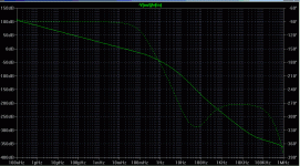
And here is the servo loop phase margin. There are 3 LF poles in the servo loop (4 including the interaction with the 5uF input coupling cap) giving a great deal of attenuation at audio frequencies.
The unity loop gain frequency of the servo loop is 18mHz. The phase margin is 94 degrees and the gain margin is a healthy 43dB. These figures do not change significantly with the input unterminated.
The unity loop gain frequency of the servo loop is 18mHz. The phase margin is 94 degrees and the gain margin is a healthy 43dB. These figures do not change significantly with the input unterminated.
Attachments
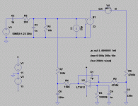
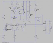
Revised clamp
Attached is a simplified schematic of some further (final) revisions I have made to the LTP diode clamp for this design.
This version does not need a trimot (which I really dislike) to balance the LTP collector voltages (which are no longer critical at all) and eliminates the clamp diodes as a possible source of non-linearity by running them (a-k) reverse biased by several hundred mV.
The limited/peak VAS current during clipping is now clamped by D2 and D5.
D1 remains as the current mirror anti-saturation clamp, which reduces the sticking time of negative rail clipping slightly.
Attachments
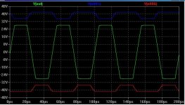
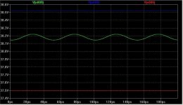
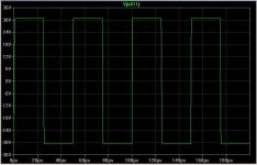
These plots show the relavant voltages across clamp diodes D1 and D2 during normal operation (in this case delivering a full amplitude 20kHz sinewave output without clipping).
The green trace is the base voltage of the emitter-follower VAS buffer Q6.
The red trace is the anode volatge of D2 (reverse biased ~700mV)
The blue trace is the cathode voltage of D1 (reverse biased ~300mV).
The green trace is the base voltage of the emitter-follower VAS buffer Q6.
The red trace is the anode volatge of D2 (reverse biased ~700mV)
The blue trace is the cathode voltage of D1 (reverse biased ~300mV).
Attachments
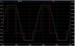
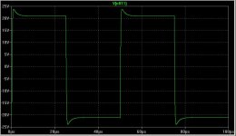
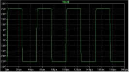
And finally, just for good measure, here is the response when driven into clipping with a 20kHz square wave. The overshoot is no longer visible as it has been chopped off,but even under these adverse operating conditions, the transient response is still as clean as a whistle.
Attachments
NFB clamp
Hi Glen,
I feel flattered that you've adopted my idea of the nfb clamp. However, you have used only the feedback part. So, I would have been even more flattered if you also had adopted the other part (which monitors Vce of the drivers), instead of adapted it.
The point is that we should prevent saturation of the drivers in a well defined/controlled manner, instead of a less exactly defined way by limiting the VAS voltage.
Also notice that in my circuit the clamping diodes are NOT directly tied to the VAS output. As a result, they hardly introduce any additional distortion.
Last but not least, my circuit doesn't need any extra active components.
I think that is a wise decision. But don't throw the baby out with the bath water. Admittedly, that Rush thingy is a PITA, but NDFL itself still has potential.
In the mean time, I've perfected the NDFL version of the Alexander amp, supplemented by CMCL, TMC and a new kind of EC (using only one additional R and two caps, dubbed ETMC). Results are very promising: simmed THD20=0.3ppm and clean clamping.
If you tie the clamping diodes to the emitters of the drivers (as I did) there is plenty of current available. But this technique is difficult (though not impossible) to apply to your design, as the CFB stage is sitting in between and your are also using elevated supply voltages for the front end.
Perhaps you may be amazed that I've abandoned the idea of the CFB OPS. The reason is that a much simpler concept (AD797 as input stage + NDFL+ETMC) is also capable of breaking the 1ppm barrier. Moreover, voltage and current clamping and EC is easier as well and simpler too, because it makes use of trannies, which are already there (VAS EF stage and CMCL stuff).
Cheers,
Edmond.
G.Kleinschmidt said:Hey!
I modified your idea for a compensated nfb clamp to adapt it to a unipolar VAS. See the attachment to post 16 here to see it added to the improved version of Cherry's NDFL amp I came up with.
Hi Glen,
I feel flattered that you've adopted my idea of the nfb clamp. However, you have used only the feedback part. So, I would have been even more flattered if you also had adopted the other part (which monitors Vce of the drivers), instead of adapted it.
The point is that we should prevent saturation of the drivers in a well defined/controlled manner, instead of a less exactly defined way by limiting the VAS voltage.
Also notice that in my circuit the clamping diodes are NOT directly tied to the VAS output. As a result, they hardly introduce any additional distortion.
Last but not least, my circuit doesn't need any extra active components.
It fixed the clipping issue, but it doesn't stop the Rush current amplifier / intergrator stage throwing a fit when the amplifier is slew rate limiting, so I abandoned the idea.
I think that is a wise decision. But don't throw the baby out with the bath water. Admittedly, that Rush thingy is a PITA, but NDFL itself still has potential.
In the mean time, I've perfected the NDFL version of the Alexander amp, supplemented by CMCL, TMC and a new kind of EC (using only one additional R and two caps, dubbed ETMC). Results are very promising: simmed THD20=0.3ppm and clean clamping.
The other issue is that the VAS must be capable of supplying enough current to drive the feedback network to reliably track an over-voltage input signal. This is a limitation when low value feedback resistors are used for low noise.
Cheers,
Glen
If you tie the clamping diodes to the emitters of the drivers (as I did) there is plenty of current available. But this technique is difficult (though not impossible) to apply to your design, as the CFB stage is sitting in between and your are also using elevated supply voltages for the front end.
Perhaps you may be amazed that I've abandoned the idea of the CFB OPS. The reason is that a much simpler concept (AD797 as input stage + NDFL+ETMC) is also capable of breaking the 1ppm barrier. Moreover, voltage and current clamping and EC is easier as well and simpler too, because it makes use of trannies, which are already there (VAS EF stage and CMCL stuff).
Cheers,
Edmond.
Yes, I'm using separate rails for the CFB OPS and the input stage/VAS, which means that the VAS clamping arrangement is a little different.
The problem with the nfb clamp and the unipolar VAS is that while the VAS transistor can supply all the current the feedback network requires on positive clipping, the current on negative clipping is limited to the VAS CCS current.
I was worried about the VAS voltage clamp referenced to the power output stage rails feeding high frequency switching spikes via the diode junction capacitances into the VAS output, but the issue is rather small and can be, for all practical purposes, completely eliminated with just some light RC filtering between the OPS supply rails and the VAS voltage clamp.
A LF pole of one hundred Hz or so is ample and the clamp will track any supply rail droop occuring with any bass transient.
Cheers,
Glen
Clamp
Hello Glenn
This circuit you have posted at, blameless input stage with TPC, Vas clamp, and CFB EC output stage can you you show me what your simulation show the amps overload recovery is without the Vas clamp.
With the more elaborate blameless front end using a buffer for the cascoded vas stage did you show much of improvement in THD performance, my sims show its very little.
Regard
Arthur
- Status
- This old topic is closed. If you want to reopen this topic, contact a moderator using the "Report Post" button.
- Home
- Amplifiers
- Solid State
- A superior VAS clamp and VAS current limit for the Blameless.