Assume if one wanted to use these boards with the original PCM63k's, that their current output +-2.1 is not enough to use the new mofsets to get these lows THD results?
Would it be worth simulating with higher supply voltages ?
Also I believe I am down for a board, want to make sure that is good for stereo balanced, if not I need 2.
Last thanks in advance for putting up with a dac neanderthal's questions")
Would it be worth simulating with higher supply voltages ?
Also I believe I am down for a board, want to make sure that is good for stereo balanced, if not I need 2.
Last thanks in advance for putting up with a dac neanderthal's questions
Just wondering if this board would work with the AD1865? I have some spare DAC END 2 boards that I have no use. DAC End 2 - the AD1865N-K with single ended vacuum output stage
Hi Guys,
Generally speaking, I would say that it's probably not worthwhile to mate this with the AD1865 or the PCM63K. It can certainly be done, but with such low output current swing, the gain has to be adjusted way up which requires larger resistor values. This in turn drops the current, which drops the transconductance and the whole thing quickly spirals downhill. The output impedance also climbs up as those resistors are increased, and you'll soon find that you need a buffer or a second stage to lower the output impedance. This basically lands you right back at the original D1 circuit, which is really what you would want to build if you had the PCM63K.
The only viable option I see would be to just drop one of those dacs in as it is, and live with the very low output. You could always add your favorite voltage gain stage after this, and that would get you what you need.
Regal: indeed, one board does provide differential stereo output and all necessary power supplies. Just add transformers and a heatsink!
Cheers,
Owen
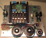
Almost ready to test the FET into the actual circuit after a weekend spent in drilling and mounting into the recycled case. Everything is mounted on a sub plate of 1/8 aluminum for better heat dissipation and easier testing. All supplies tested ok. I'll mount the FET on the bottom plate near the heatsink for the test.
Attachments
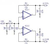
no, the pots on the PCB are a completely different purpose, simply to adjust gate bias to match AVCC/2 on your particular dac. so power up your buff and measure what the DC voltage from AVCC L/R reg to ground is and divide that by 2 (normally around 1.65-1.7vdc), note that down, power up the board with the dac not connected and adjust all the pots to match that voltage on each mosfet source ->G. power down and install the dac, power the lot up, measure each source to ground and readjust to match the voltage again as it will change a touch under load.
hope that makes sense
hope that makes sense
Last edited by a moderator:
oops...., yes source, now that was a brain fart; i started thinking of matching too even after mentioning these were already set. its best to measure the reg rather than assuming 3.3/2 as the tp boys at least with the buf 2 onwards increased this voltage to 3.4 and even a touch higher on some modules. I have gone as far as 3.6v in my experiments; Dustin gives this tip to increase DNR; but i'm not sure if they were doing it back then; sorry i forgot you were using the V1 dac.
Last edited:
Exactly what he said ^
The chassis looks great, and again, kudos on putting in all the extra work to etch your own board! I'm looking forward to hearing your impressions.
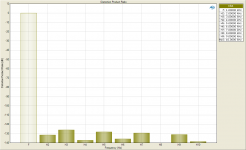
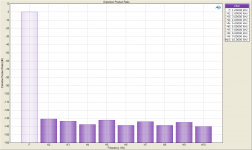
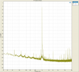
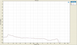
I recently took a few more measurements of my NTD1 using a separate outboard ADC and patching it digitally into the AP. This allows more accurate measurements as the outboard ADC has much lower distortion than the internal one on the AP.
As I always suspected, distortion is significantly lower than originally measured.
Remember this post?
http://www.diyaudio.com/forums/digi...ssic-pass-labs-d1-ess-dac-13.html#post2187211
Compare and contrast to the graphs attached below:
1. DPR @ -4dBFS - 2nd and 3rd harmonics are down 131dB and 127dB respectively
2. DPR @ -6dBFS - 2nd and 3rd harmonics are down 131dB and 133dB respectively
3. FFT of the output @ -6dBFS. Scale the whole thing up by 12dB if you want values in dBV. This puts the noise floor at between -138dB and -158dB!
4. THD vs. Freq @ -6dBFS. Values below 10Hz and above 7kHz are not valid due to high and low pass noise filters at 20Hz and 22kHz.
Hopefully that's some encouragement to get your project finished!
Cheers,
Owen
The chassis looks great, and again, kudos on putting in all the extra work to etch your own board! I'm looking forward to hearing your impressions.
I recently took a few more measurements of my NTD1 using a separate outboard ADC and patching it digitally into the AP. This allows more accurate measurements as the outboard ADC has much lower distortion than the internal one on the AP.
As I always suspected, distortion is significantly lower than originally measured.
Remember this post?
http://www.diyaudio.com/forums/digi...ssic-pass-labs-d1-ess-dac-13.html#post2187211
Compare and contrast to the graphs attached below:
1. DPR @ -4dBFS - 2nd and 3rd harmonics are down 131dB and 127dB respectively
2. DPR @ -6dBFS - 2nd and 3rd harmonics are down 131dB and 133dB respectively
3. FFT of the output @ -6dBFS. Scale the whole thing up by 12dB if you want values in dBV. This puts the noise floor at between -138dB and -158dB!
4. THD vs. Freq @ -6dBFS. Values below 10Hz and above 7kHz are not valid due to high and low pass noise filters at 20Hz and 22kHz.
Hopefully that's some encouragement to get your project finished!
Cheers,
Owen
Attachments
Great distortion figures. But I'm not too nervous about perfect tech specs. My Aleph30 clone made years ago is still one of my preferred amp, and doesn't test so great. I have a CLIO analysis system and I'll certainly have a look at the specs, but I'll be happy if the dac sounds just great
well get ready to be happy
Yes Dire Straits "Iron Hand" Playing right now Thru Owen's D1...scary good! Me Happy!
Thanks Again Owen.
igwt
I added a shunt reg between the on-board regulator and buffalo ll.
With distortion levels so low from source to output tweaks are audible ,this one
seems to be a positive one to my ears.
My NTD1 Bll combo does not suffer from what I call "digitosis"...you know the junk that makes some of Madeleine Peyroux's recordings fatiguing and sends your tweeters into fits on a most digital systems. I think reviewers call it "glare" Well the glare is gone! Analog tone with digital detail.
igwt
Hi. I may doing something wrong. The DAC VA/2 = 1.64V, and can be easily measured at the output of the Buffalo DAC output (nothing connected).
Then without connecting the DAC, I adjusted all four D1 FET gates to the same voltage of 1.64V, easily done.
I connected the DAC it is was very wrong. The DAC Vd and Va where drag lower than normal, VD was 4.52V instead of the normal 5V, the DAC stop to works, and the DAC outputs where stuck at -0.7V.
If I change to D1 FET Gate until the DAC sees 0V at its output, it is working again, at this point the FET Gate voltage is about 3.3V.
With the D1 pot I can vary the DAC output voltage (connected to the D1) from -0.7V to +0.7V only, not the expected 1.64V.
It is if like the protection zener are conducting at 0.7 and not 3V.
Remember, I'm using my own PCB. It can still be wrong. I already found and corrected a few mistakes.
Any idea? Anything to test?
Thanks...
SB
This could be a few things:
1. The gate voltage is not what you should be measuring! You need to adjust the pots to measure 1.65VDC on the SOURCE of the mosfet (where the DAC outputs connect to) relative to GND.
2. The protection zener diodes were incorrect on the PCB. This error has been covered several times throughout the thread, but it's easy to miss. If you want to keep the protection zeners, you need to make a little tee-pee putting two zeneres back to back on the same pad. There are instructions in the thread somewhere with pictures.
Fix the above two things, and you should be good to go. Do not attach the DAC to the I/V stage until you've got the proper 1.65VDC at the source of each fet! If you have a high voltage there, you could damage the DAC.
Regards,
Owen
- Status
- This old topic is closed. If you want to reopen this topic, contact a moderator using the "Report Post" button.
- Home
- Source & Line
- Digital Line Level
- A New Take on the Classic Pass Labs D1 with an ESS Dac