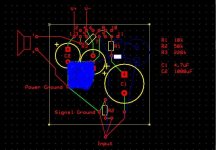
S.C.,
Instead of trying to explain, I did some mods to your circuit, I hope it's clear enough.
They are in blue.
You should join the two PSU caps, don't run wires around.
With these changes you'll get around half the board size, and a much better layout.
Instead of trying to explain, I did some mods to your circuit, I hope it's clear enough.
They are in blue.
You should join the two PSU caps, don't run wires around.
With these changes you'll get around half the board size, and a much better layout.
Attachments
Nuuk said:What's that blue thing? Portuguese censorship")
That blue thing means that S.C. should join the two caps to make a ground star.
The way he had, with wires going back and forth to a "ground" point is not a good thing to do.
So, it's censured.
That blue thing means that S.C. should join the two caps to make a ground star.
Yes, I agree, I hadn't noticed that before. Must be the heat

Nuuk said:
Yes, I agree, I hadn't noticed that before. Must be the heat
Yesterday in the news they were saying it has been hot in the UK.
30º C!
And it's raining here.

carlosfm said:S.C.,
Instead of trying to explain, I did some mods to your circuit, I hope it's clear enough.
They are in blue.
You should join the two PSU caps, don't run wires around.
With these changes you'll get around half the board size, and a much better layout.
Did I do that already on my 3th and 4th edition? There are 5 pics on that site. I will still refine it, but I just curious.

The right way
S.C.,
I have to give you sincere congratulations.
You investigated, made a layout of your own and before doing anything you asked if that was OK.
Now you're going to do your GC.
We are here to help, always feel free to ask.
It's better to do the way you did than an unexperienced person end up with a cap blown in his face.
Re: The right way
Thx carlosfm, I hopw I didn't annoying you guys about stuffs. I always ask some much, cuz I don't trust myself. It just like I always check the ans before I move on to next calculous question.


carlosfm said:S.C.,
I have to give you sincere congratulations.
You investigated, made a layout of your own and before doing anything you asked if that was OK.
Now you're going to do your GC.
We are here to help, always feel free to ask.
It's better to do the way you did than an unexperienced person end up with a cap blown in his face.
Thx carlosfm, I hopw I didn't annoying you guys about stuffs. I always ask some much, cuz I don't trust myself. It just like I always check the ans before I move on to next calculous question.
Damn, nice things always come at last. The final one is out ! 5th edition. The Ground under Cap really help me allot! Thx again for eveyone who helped me in this tread. http://hk.geocities.com/solomon_choi/GC2.html
P.S Partsconnxion.com just charged me, that's mean I need to wait about a week to begin all this. T_T
P.S
Partsconnxion.com just charged me, that's mean I need to wait about a week to begin all this. T_T same link.
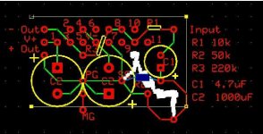
Hi S.C. I second what Carlos said about your sensible approach to building your GC!
I have looked at V6 and there is just a little bit more tidying up that I would do.
On the signal input, I presume that the circle shown off the PCB is the input phono socket. You show three wires coming from that to the PCB but you only need two.
The wire carrying the signal goes to a hole and then to R2 but you can also just put a track from that hole straight to the + terminal of C1. That means that you do not need the other wire carrying the signal to the PCB.
Finally, if you initend to earth any casework, you should do it via a 100R resistor with a small capacitor in parallel so you may wish to make provision for those items on the board. I would suggest they would be best put in on the bottom of the board near MG. The PCB would need to be made a little bigger but it is so small anyway, that will not be a problem.
Nuuk said:Good morning CFM!
That's a good idea but I would move the resistor SE a little to make sure it clears the caps. And you still don't need the two signal connections to the phono socket.
Good morning Mr. Decibel.
Yes, well... I didn't do better bacause I had to delete part of the sketch.
Let's see what S.C. makes now, I think he got the piccture.
Good morning Nuuk, and Carlosfm,
I did the change, but now I'm doing a realiztic check. The resistior is kindla big. I rather need to change the layout to a little bit bigger or just simplly cut the un used led of LM3875TF. Which opion do you guys prefer? On the earthing case thing, is it I just connect the PG to a 100 Ohm resistor and a Cap (can it be 16v?) than to the MG or the case?
I did the change, but now I'm doing a realiztic check. The resistior is kindla big. I rather need to change the layout to a little bit bigger or just simplly cut the un used led of LM3875TF. Which opion do you guys prefer? On the earthing case thing, is it I just connect the PG to a 100 Ohm resistor and a Cap (can it be 16v?) than to the MG or the case?
DON'T DO THAT
the pins of the LM3875 are not aligned the way you have them -- I guess you are using the freeware from www.expresspcb.com )there is a 3.4 mm (about 1/8th inch) space between the odd OR even pins as seen horizontally. They are spaced about 400 mills front to back.
They don't exactly fit on the expresspcb grid. Before you have your proto's burned, print out and make sure the parts fit.
In ultiboard I designed a custom device for the PCB layouts I use. Note also -- the width of the pins on these devices is a bit larger than a DIP IC -- you will have to specify
take a look at page 17 of the PDF from National.
- Status
- This old topic is closed. If you want to reopen this topic, contact a moderator using the "Report Post" button.
- Home
- Amplifiers
- Chip Amps
- A GC Layout check.