Move the feedback closer to the opamp... ok, no problem...
My thinking, as to why it's in it's current position, was to minimize sources of interference, such as the high voltage signal from the output, traveling across the board...
But alas, I see instead of reducing interference, I have created a receptor for just what I was trying to prevent...
Modify low voltage PS... if it doesn't flow thru the star, where does it flow to/thru??
As for bias stability, I understand what your talking about.. but I don't have the experience and/or knowledge to comment... for simplicity and space, I left it off the heatsink...
Thanks!!!
Yes, as that is one of the most sensitive nodes in the circuit it should be kept localized to the opamp. The trace running right above it now is already connected to the output. ")
The thing with the LV PS: The peaky currents between transformer center tap and filter caps flow through the star point. It could be improved - but it is probably okay as these are pretty small.
Driver transistor ground to star - don't forget that one. After moving the feedback resistors and combining regulator and bypass ground there should be a place to route it.
Oh, I forgot: Both positive and negative regulator and decoupling should be connected through the same trace back to star to make effective decoupling for the opamp. Inductance in the local opamp power supply loop should be minimized.
megajocke said:Yes, as that is one of the most sensitive nodes in the circuit it should be kept localized to the opamp. The trace running right above it now is already connected to the output.
The thing with the LV PS: The peaky currents between transformer center tap and filter caps flow through the star point. It could be improved - but it is probably okay as these are pretty small.
Driver transistor ground to star - don't forget that one. After moving the feedback resistors and combining regulator and bypass ground there should be a place to route it.
Oh, I forgot: Both positive and negative regulator and decoupling should be connected through the same trace back to star to make effective decoupling for the opamp. Inductance in the local opamp power supply loop should be minimized.
Good call. I almost suggested using a single ground return for both regulators and the opamp decoupling, but somehow didn't get around to it, and instead mentioned putting caps between regulator output and ground pins. But now, with the regulators nice and close to the opamps and the grounds combined, the opamp's local electrolytic reservoir/decoupling caps should be able to also serve as the regulators' output caps.
Ideally, I guess, the HF decoupling path between the two opamp power pins should be as short as possible, meaning that ideally the two 0.1uF decoupling caps would connect to ground very close to each other. If that seems to be a problem, later, I guess a 0.1uF or so cap could be tacked on, under the board, diagonally from one opamp power pin to the other.
krazatchu said:Holy cow!
There is so much to learn!!
Same here! Sometimes I feel like I've just barely scratched the surface, so far, but am hoping that that's wrong and that some point of 'critical mass' is close to being reached.
But I also feel like I was over halfway there, already, when I first started even thinking at all about the need for things like star grounding.
That might be a good example of 'things they didn't mention in EE school'. But at least they did provide the tools needed to analyze and understand it.
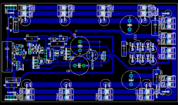
Change log... Version 23
1) Merged grounds for:
+ Regulator GND
+ Regulator decoupling caps / opamp caps
- Regulator GND
- Regulator decoupling caps / opamp caps
2) Opamp decoupling caps GND as close as possible
3) Moved main feedback components as close as possible to opamp
4) Merged grounds for:
Opamp input GND
Unused opamp input
R14 feedback GND
5) Put LV PS main caps to center tap, before start ground, to reduce hum
6) Added driver transistors GND (R8/C5, R9/C6) to star GND
7) Rotated bias transistor and components for better packing, moved opamp left...
8) Moved parallel (100uf, 100nf) caps to the right, closer to power rails input...
Pic included...
Thanks!!
Attachments
Change log... Version 23
1) Merged grounds for:
+ Regulator GND
+ Regulator decoupling caps / opamp caps
- Regulator GND
- Regulator decoupling caps / opamp caps
2) Opamp decoupling caps GND as close as possible
3) Moved main feedback components as close as possible to opamp
4) Merged grounds for:
Opamp input GND
Unused opamp input
R14 feedback GND
5) Put LV PS main caps to center tap, before star ground, to reduce hum
6) Added driver transistors GND (R8/C5, R9/C6) to star GND
7) Rotated bias transistor and components for better packing, moved opamp left...
8) Moved parallel (100uf, 100nf) caps to the right, closer to power rails input...
Pic included...
Thanks!!
Attachments

Off-topic:
Hey megajocke,
Could you please take a look at this thread:
http://www.diyaudio.com/forums/showthread.php?s=&threadid=116374
I think I have mucked things up, there. Your expertise is needed.
I'm sorry for the off-topic post. I couldn't email directly.
- Tom
Hey megajocke,
Could you please take a look at this thread:
http://www.diyaudio.com/forums/showthread.php?s=&threadid=116374
I think I have mucked things up, there. Your expertise is needed.
I'm sorry for the off-topic post. I couldn't email directly.
- Tom
It looks nice.
I'd sneak the feedback trace under C12 or C7 all the way to the output terminal block for least distortion and then widen the traces connecting the emitter resistors of the outputs. Copper wires can be soldered to the traces if needed to reduce resistance even more if the outputs don't share current good enough. How wide are the traces now and what is the copper thickness of the board?
I'd sneak the feedback trace under C12 or C7 all the way to the output terminal block for least distortion and then widen the traces connecting the emitter resistors of the outputs. Copper wires can be soldered to the traces if needed to reduce resistance even more if the outputs don't share current good enough. How wide are the traces now and what is the copper thickness of the board?
Woot!
I had thought of something similiar, running the feedback seperately...
Then I thought, if it's included in the zobel network, then it would be filtered and hence be "cleaner" ...
So I split it from the parallel caps, all the way back to the connector...
See pic... Am I right, wrong?
As for the coper thickenss of the board.. I don't know, it's not labeled... I can pick up something heavier next time I'm at the market...
The traces, specifically the ones connecting the resisitors to the emitter of the driver, are currently 3.81mm...
Edit: I jsut made the previously mentioned traces 6.4516 mm..
Thanks!!
Attachments
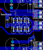
That looks fine. From the zobel or from the output terminal shouldn't make any difference. It's the ugly current from the decoupling caps that should be avoided. The splitting solves this
It's just that traces with the resistors that might need lower resistance. The rest of the board won't care - resistance for 10cm length, 6.4516mm width and 0.035mm thickness is about 0.007ohms. It might make a difference for the emitters though - it's about 10% of the parallelled value of these resistors. The cross section is 0.23mm^2 so even a 0.5mm^2 copper wire soldered on will make it very low.
It's just that traces with the resistors that might need lower resistance. The rest of the board won't care - resistance for 10cm length, 6.4516mm width and 0.035mm thickness is about 0.007ohms. It might make a difference for the emitters though - it's about 10% of the parallelled value of these resistors. The cross section is 0.23mm^2 so even a 0.5mm^2 copper wire soldered on will make it very low.
Dirty Harry again
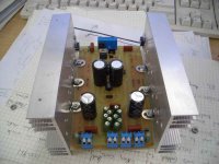
×áæïðáñôáëå, take this hard checked project of AB class which can produce 350W/8ohms or 650W/4ohms. You can also increase the supply to +/-86Voltsdc without fear so you can take 420W/8ohms or 780W/4ohms. Attention!! only one channel is shown in photo. You can bridge two channels to break the glasses in your house and to meet your neighbours! And the police!
×áæïðáñôáëå, take this hard checked project of AB class which can produce 350W/8ohms or 650W/4ohms. You can also increase the supply to +/-86Voltsdc without fear so you can take 420W/8ohms or 780W/4ohms. Attention!! only one channel is shown in photo. You can bridge two channels to break the glasses in your house and to meet your neighbours! And the police!
An externally hosted image should be here but it was not working when we last tested it.
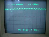
Do you have any pictures? We want to see your amp That stuff looks like 40kHz, and that's pretty low. Did it go away when using the 5548? (4558?) Does it change with O/P bias current? There shouldn't be any oscillation at all in an amp unless it is a self oscillating class D amp.
That stuff looks like 40kHz, and that's pretty low. Did it go away when using the 5548? (4558?) Does it change with O/P bias current? There shouldn't be any oscillation at all in an amp unless it is a self oscillating class D amp. 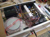
- Status
- This old topic is closed. If you want to reopen this topic, contact a moderator using the "Report Post" button.
- Home
- Amplifiers
- Solid State
- ~700w ampifier