A list of Modifications...
1) Regulators change to TO-220
2) Regulator output caps 25uF electro
3) Opamp decoupling caps 0.1uf
4) C2, opamp feedbackcap, 100pF
5) C3, main feedback cap, 22pF
6) opamp change to 4558
7) add caps to driver boards, 100uF and 100nF, parallel to 22,000uf
8) change input as per Gootee's suggestion..
9) separate input ground...
The only part that confuses me is #9... Wouldn't this leave he input floating? Shouldn't the input ground be conected to the ground of the opamp supply??
Should I separate the low voltage gnd and high voltage gnd with a resistor? I think I read that somewhere about gnd topologies...
Thanks!!
Michael
EDIT: regarding item 7, I just noticed, as I was adding the mods to the schematic...
In post 151, Gootee says two caps from power rail to ground,
And in post 169, Megajocke says two caps from power to output...
Should I do both? or is there some mistake?
As per item number 7...
Simulation shows that the two caps can't be from power rail to ground...
So, I'm assuming Gootee meant from the same as Megajocke... from power to output, parallel to the 22,000uF but on the board...
Thanks!!
EDIT: I had already performed this mod from power to GND, after I changed the burnt transistors... And I was wondering what hte problem was, I figured it to be another burnt compnent, but it seems it might be the caps I added...
Well, I posted a reply shortly after your last post. But it seems to have not made it to the forum.
Sorry about the confusion on my part, about #7, I had forgotten about the 'odd' power supply vs amp topology. I meant that the local/on-board caps should be parallel to the caps at the other ends of the wires.
Regarding #9:
I only meant that the bypass caps' ground-return currents should share as little conductor as possible with the input and feedback ground-return. They will both return to the same place, just not in/on the same conductor. (See 'star ground'.)
If they DO share the same ground-return trace, then, when the bypass caps' dynamic return currents induce a nasty-looking dynamic voltage across the parasitic inductance and resistance of the ground-return trace (or copper area, if shared), that induced voltage will be arithmetically added to the input signal (because that induced voltage will be modulating the input's ground-reference point's voltage).
Not only does that muck-up the input signal. It is also a kind of feedback, and can cause oscillations.
Of course, if the trace-lengths are small-enough, it might not be worth worrying about any of that. (However, remember that the voltage induced across the inductive portion of the trace's parasitic impedance would be L(di/dt), which could get relatively large compared to R x i, even for small L and i, if i is dynamic-enough.)
Another point: It might be a good idea to run the regulator's reference ground to the opamp's bypass caps' ground as a separate trace, i.e. run it separately from the main ground-return trace that comes from the opamp's power supply's smoothing caps, for the same sorts of reasons as above, i.e. keep the main return currents out of the ground-voltage-sensing trace.
You could make the boards so it's possible to insert a resistor between input ground and the rest of the ciruit. Only R1 and R14 and input shield should connect to this. If you separate the low and high voltage grounds then the driver currents will flow through the separating resistor and cause bad behaviour. The separation is probably not needed though. Just following standard grounding practice could be bad due to the unusual topology.
Something that might be very important is the connection of ground to chassis - capacitance of the transformer will cause ground bounce otherwise and possibly HF oscillation. The ground should be connected to chassis just outside the high current loops to prevent modulation of ground potential due to speaker currents. The opamp circuit ground is also connected to this point.
I think you should skip the idea of several boards, getting the current paths right seems like a hard problem. I'd keep driver transistors on board and connect the power transistors with wire. B, C and E of each transistor should be twisted or at least kept close together.
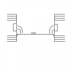
Something like this:
Something that might be very important is the connection of ground to chassis - capacitance of the transformer will cause ground bounce otherwise and possibly HF oscillation. The ground should be connected to chassis just outside the high current loops to prevent modulation of ground potential due to speaker currents. The opamp circuit ground is also connected to this point.
I think you should skip the idea of several boards, getting the current paths right seems like a hard problem. I'd keep driver transistors on board and connect the power transistors with wire. B, C and E of each transistor should be twisted or at least kept close together.
Something like this:
Code:
                  optional input gnd
                  separation resistor      speaker return
                       |                       |
                       |     opamp             |      HV center tap
                       |    circuit gnd        |          |
                       |    and LV PSU gnd     |     filter capactiors centerpoint
                       |    and driver         |          |
                       |      transistors      |          |
                      \ /      |               |          |
                               |               |          |
input shield ----*----|===|----*--------*------*-----*----*
                 |                      |            |
                 |                      |            |
       feedback resistors             chassis   transistors
gnd and decouplingJust because the circuit is drawn with the collectors of the outputs at ground potential doesn't mean that you should mount them to the chassis.
QSC and Crown mount their TO-3 cased outputs directly to the heatsinks, which are then isolated from the chassis. A chassis makes a poor high current ground.
"capacitance of the transformer will cause ground bounce otherwise and possibly HF oscillation. "
Post #26
The power transformer needs to be a low-leakage type. The QSC has a screen over the primary, and another between the two secondaries.
Darn, I forgot to mention an input ground separation resistor.
It would be good to at least make some pads for one, which you could jumper with wire, otherwise. Actually, if the grounding is properly designed (i.e. with full 'star grounding', you "shouldn't" need one. So I'd put one in, just in case.")
(I think) The idea is that if the opamp's input ground reference point is connected to a ground point with a varying voltage, the ground separation resistor might have enough voltage drop that the input ground reference's voltage will be above the peak of the varying downstream ground's voltage, which would keep the input ground reference's voltage from varying (and also keep the currents in the downstream ground from flowing into the reference ground node).
The input ground separation resistor is usually quite small, typically from one to several Ohms.
It would be good to at least make some pads for one, which you could jumper with wire, otherwise. Actually, if the grounding is properly designed (i.e. with full 'star grounding', you "shouldn't" need one. So I'd put one in, just in case.
(I think) The idea is that if the opamp's input ground reference point is connected to a ground point with a varying voltage, the ground separation resistor might have enough voltage drop that the input ground reference's voltage will be above the peak of the varying downstream ground's voltage, which would keep the input ground reference's voltage from varying (and also keep the currents in the downstream ground from flowing into the reference ground node).
The input ground separation resistor is usually quite small, typically from one to several Ohms.
Well, I took the caps off that I added from rail to gnd...
I thought I might not have to make a new board....
However, now I'm getting alot more oscillation than I had before....
seems to be less with the tl072, but still not good... around 25Vp
I haven't picked up the ne4558 yet...
I tried grounding everything to a single point, but that didnt make a difference....
I think it's time to start over... this board has become a bit of a mess... good learning experience however...
I will, in addition to the previous 9 items...
10) Isolate the heatsink from the case...
11) Use a star ground topology
Now to decide, what layout...
Wow. I guess you really WERE listening. Cool.
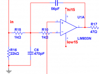
I can't really decipher the area around the opamp, too well. Sorry. I guess my eyes are getting worse than I thought.
But it looks like C1 and C2 are connected, which might mean that the resistor that was added between the junction of R1/C1 and the inverting input was omitted.
Also, I don't see the connection from R2, C1, and R14 to the star ground, which is also where you could leave pads for an optional ground-separation resistor (wire jumper if not used). Oh wait, I see it now, I think. R14's is separate, way on the right. And R2/C1's goes under the resistor behind the regulator. I guess you might want to break both of those paths and make pads for two ground-separation resistors. Then again, you could always just cut them later, and 'surface mount' some resistors, if it became necessary.
I can't see it well-enough to check a lot of the rest of it.
It looks like C2 doesn't go straight from the output pin to the inverting input pin. So is the added resistor, that I thought was omitted, stuck in there, accidentally? Or is that how you want it wired? In my schematic, the input connects to R1, then C1 goes to gnd, then there's the added resistor, then C2's junction with the opamp's neg input.
Also, there should be another small electrolytic capacitor for each regulator, from each regulator's output pin to its ground pin.
Also, there should be another small electrolytic capacitor for each regulator, from each regulator's output pin to its ground pin.
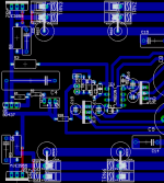
Going to try and post it as a pdf...
I added/changed....
fixed input...
item 7, parallel caps on board, not as close as they should be to the right side...
added vias and wires, 6 of them...
added electro' caps from regs output to regs gnd...
moved regs closer to opamp...
A few notes, in case anyone was wondering...
a)The connectors for the output transistors will not be used, I just used the footprint for convienince...
b)The resistors above and below the previously said connectors, will not connect to the connectors... but will connect to the transistors
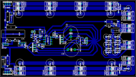
Is there anything I might have put too close? wires, components, etc.. that might cause interference?
Edit: pdf too big, will add it in two parts... left and right... original size is 1805 wide x 1000 high...
I added/changed....
fixed input...
item 7, parallel caps on board, not as close as they should be to the right side...
added vias and wires, 6 of them...
added electro' caps from regs output to regs gnd...
moved regs closer to opamp...
A few notes, in case anyone was wondering...
a)The connectors for the output transistors will not be used, I just used the footprint for convienince...
b)The resistors above and below the previously said connectors, will not connect to the connectors... but will connect to the transistors
Is there anything I might have put too close? wires, components, etc.. that might cause interference?
Edit: pdf too big, will add it in two parts... left and right... original size is 1805 wide x 1000 high...
Attachments
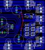
You should move the feedback resistors closer to the opamp to minimize capacitance at its inputs. Also you might want to reconnect the low voltage power supply so that it's center tap current doesn't flow through the star.
I'm wondering what is needed for bias stability for this amp - does the bias transistor need to be on the same heatsink as the drivers? I guess it isn't very critical if it is biased in AB+B but if running quiescent current through outputs it might be needed.
I'm also worried about the connection of the emitters of the driver transistors to a dirty ground and the loop around the card. I'd say:
1. Move C3, R15 and R14 to the empty space above the opamp. The ground trace that goes to input is perfect for R14.
2. Ground of R8//C5 and R9//C6 to star ground instead of making that scary loop around the card.
3. Optimally charging pulses for LV power supply should be kept out of star ground - but the worst that can happen is a little hum so this isn't very important.
4. Don't use separate ground returns from the regulators and their output decoupling. This leaves some more space for driver returns. The noninverting input of the unused opamp doesn't need it's own return either, connect to the ground just below.
The connection between clean star and dirty ground looks like it might work. Chassis should probably be connected to the GND terminal block together with speaker return to eliminate ground bounce due to capacitive currents from the output throught the transformer.
- Status
- This old topic is closed. If you want to reopen this topic, contact a moderator using the "Report Post" button.
- Home
- Amplifiers
- Solid State
- ~700w ampifier