More progress...
I think a separate PSU board is the best route, just to keep this simple, and to keep options open. Still to be decided, but if I don't include one on here I'll make a small companion board with solid state rectification and the mosfet ripple filter. Still need to move things around a smidge here and there, but I'm liking it so far. Once I like it I'll double it to the second channel.
I think a separate PSU board is the best route, just to keep this simple, and to keep options open. Still to be decided, but if I don't include one on here I'll make a small companion board with solid state rectification and the mosfet ripple filter. Still need to move things around a smidge here and there, but I'm liking it so far. Once I like it I'll double it to the second channel.
Attachments
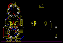
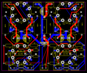
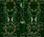
Current draft, with basic RC onboard CRC filter. Screw terminal headers for input L/GND, R/GND, LFB/GND, RFB/GND, PWR/GND OUt, PWR/GND IN, and outputs for the output transformers. Managed to fit it all on a 100mm x 120mm board. Still need to fix silk screen part names, add mounting holes, filament wire holes/pads, and waiting for some suggestions. I tried to make it as close to a star ground per channel as possible.
I also need to draw up a nice schematic (any volunteers?!) so that I can give everything solid parts names to refer to.
Slowly but surely I'm getting something together, and it'll take a bit of polish but I'm liking it so far.
Unfortunately I don't think that the 6AS7 will fit nicely (well, it will be really cramped at the very least) but I plan on doing another version with nine-pin input tubes for the front end as well, so that might buy us some more room, otherwise I would have to increase the board size considerably to space everything out to accommodate the big coke bottles.
Attachments
Last edited:
Alright, I think the layout is more or less good.
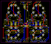
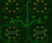
I went ahead and moved the output sockets closer to the top of the board, went with bigger coupling caps, rearranged a few connections, and spaced some things out a bit more. I think that big boy triodes like the 6AS7G will fit a bit better now, although it still may be a little tight. Might need to go for the 6080 type of bottles if it's too close for comfort... I'll have to do a quick mockup tonight after I get home to see how cramped it really is though. If they fit it would be pretty easy to simply run bigger garter resistors off board to use the big bottles, which would make for a very compact stereo board for a good 7~8 watts per channel!
Ignore the obvious error at the bottom middle connector (power and ground shorted to the left pin) and the silkscreen being funky for now. I need to rearrange and rename the parts designations, copy some of the silkscreen to the bottom side of the board, and maybe put a larger footprint part outline under the concertina socket to accommodate physically larger capacitor types in that location. Then I'm going to measure it out and move things around so that they line up as close to perfect with the board outline as possible, as the grid is off by a small amount from the actual dimensions. Current board size is still 100x120mm, pretty compact")
So far the plan is to mount all the resistors on the top with the sockets, and the capacitors will all go on the bottom, as will the screw terminals. Since its all plated through hole you can put any components on either side so long as they fit. Should be nice and versatile. I tried to make the layout the same on both sides to make it easy to follow for novice builders too.
Seems to have gone quiet around here lately, so I'm still waiting for some suggestions before I truly finalise any ideas.
I went ahead and moved the output sockets closer to the top of the board, went with bigger coupling caps, rearranged a few connections, and spaced some things out a bit more. I think that big boy triodes like the 6AS7G will fit a bit better now, although it still may be a little tight. Might need to go for the 6080 type of bottles if it's too close for comfort... I'll have to do a quick mockup tonight after I get home to see how cramped it really is though. If they fit it would be pretty easy to simply run bigger garter resistors off board to use the big bottles, which would make for a very compact stereo board for a good 7~8 watts per channel!
Ignore the obvious error at the bottom middle connector (power and ground shorted to the left pin) and the silkscreen being funky for now. I need to rearrange and rename the parts designations, copy some of the silkscreen to the bottom side of the board, and maybe put a larger footprint part outline under the concertina socket to accommodate physically larger capacitor types in that location. Then I'm going to measure it out and move things around so that they line up as close to perfect with the board outline as possible, as the grid is off by a small amount from the actual dimensions. Current board size is still 100x120mm, pretty compact
So far the plan is to mount all the resistors on the top with the sockets, and the capacitors will all go on the bottom, as will the screw terminals. Since its all plated through hole you can put any components on either side so long as they fit. Should be nice and versatile. I tried to make the layout the same on both sides to make it easy to follow for novice builders too.
Seems to have gone quiet around here lately, so I'm still waiting for some suggestions before I truly finalise any ideas.
Attachments
Last edited:
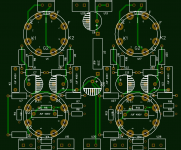
I wouldn't mind adding a hole on either side of each socket, that way the board could be mounted to a top plate via standoffs so that there was some additional support. If anything those would serve as the main mounting holes for the board that way.
Good suggestion, I hadn't actually even thought of that before you mentioned it! Shows how much of a noob I am at this
I'm going to thicken the ground traces under the output tubes cathode/capacitors too, to be able to handle the higher current uses that may come up too.
Good suggestion, I hadn't actually even thought of that before you mentioned it! Shows how much of a noob I am at this
I'm going to thicken the ground traces under the output tubes cathode/capacitors too, to be able to handle the higher current uses that may come up too.
Last edited:
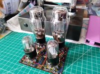
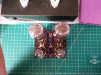
So, with a printout of the current state of the board, I dug out a pair of 6N13S (Russian 6AS7G) and did a quick mockup. It'll be a tight fit, but they fit! Personally, I wouldn't have a problem running a pair on this board, so long as a few ventilation holes were put all around the socket.
Kind of makes me want to build up a six channel amplifier using three boards for home theatre system use
Kind of makes me want to build up a six channel amplifier using three boards for home theatre system use
Attachments
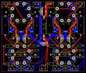
The only area that I was a bit concerned on that at first was the plate traces, and I reduced some of the traces that go between pins down to .5mm just to get a bit more clearance. I'm going off of the common practices I see on other boards I've worked with (such as the now famous "red board" from Pete Millett) and trying to keep the higher volt stuff on the opposite side of the other traces to be sure. As I said, I'm sort of a noob at this, so any suggestions are welcome.
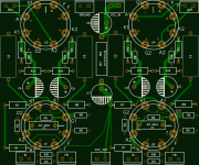
Added some mounting holes to either side of each socket, thickened the grounds at the outputs, and did a bit more cleanup.
Added some mounting holes to either side of each socket, thickened the grounds at the outputs, and did a bit more cleanup.
Attachments
Last edited:
More fiddling. I've turned this into sort of my personal developement blog of sorts!
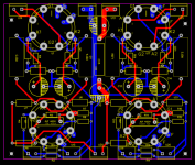
As far as I can tell, I've got pads on each side, it may be the default way that easyEDA does things for plated through hole? Going to fix the silkscreen, then I'm trying to figure out how to bulk copy all the parts names and outlines to either side to make it easier to tell what's going on, but it looks like I may have to do it manually... Still figuring it out.
As far as I can tell, I've got pads on each side, it may be the default way that easyEDA does things for plated through hole? Going to fix the silkscreen, then I'm trying to figure out how to bulk copy all the parts names and outlines to either side to make it easier to tell what's going on, but it looks like I may have to do it manually... Still figuring it out.
Attachments
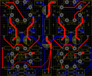
Fixed the silk- But I still can't get it to copy to the bottom without going one by one without making custom parts outlines apparently. I'm not sure if i want to go through and Label the bottom placement all one at a time, as it's pretty trivial to go through while populating the board and verify placement while you go. As it is now when i go to add more silk on the bottom, the render/preview gets all funky and throws some of the labels off of the board, and I'm unsure if this is either a design error on my part, or a rendering bug for the preview feature. If I can't figure it out I may just leave the bottom silk extras out.
(EDIT-Figured out the bug, I just had to scoot them all over a bit and now they render fine...)
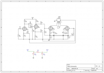
(EDIT- also included a current schematic.)
(EDIT-Figured out the bug, I just had to scoot them all over a bit and now they render fine...)
(EDIT- also included a current schematic.)
Attachments
Last edited:
So, with a printout of the current state of the board, I dug out a pair of 6N13S (Russian 6AS7G) and did a quick mockup. It'll be a tight fit, but they fit! Personally, I wouldn't have a problem running a pair on this board, so long as a few ventilation holes were put all around the socket.
Kind of makes me want to build up a six channel amplifier using three boards for home theatre system use
Definitely looks tight for 6AS7/6N13S but it should work. As you say, good ventilation would be a good idea. You've said something about it already but I wasn't clear, would the garter resistors be mounted on the board of off-board? That would be another issue for heat dissipation, particularly using 6AS7 family.
Yeah, they would need to be off board, otherwise the board would need to be much, much bigger, seeing as the primary focus was for the 6SN7, I made the footprints for the cathode resistors 1/2W... If it was me I would use either TO-220 or aluminum chassis mounted resistors for that application, and run them off board to the top plate of the amplifier, or even run a set on tag strips underneath the board. In most applications you won't be running them too hot though, 200mA@64V gives 12.8Watts per resistor array, which is a good bit of heat but not too bad, assuming you go for the 100V/100mA/-32V operating point, off of a 165V power stage supply. I plan on at least one build using the 6N13S, and will go that way for one for sure.
If I like how these boards turn out I will start on a version using the EL84/EL86 that will be split into two 100x100mm boards, with larger onboard footprints for garter resistors, and a few surprises for the input stage (CCS plate load option for the input stage, LED option for its cathode, etc) and maybe also a small universal input/concertina board, meant to be used with multiple output tube types that will be mounted off board on separate sockets...
If I like how these boards turn out I will start on a version using the EL84/EL86 that will be split into two 100x100mm boards, with larger onboard footprints for garter resistors, and a few surprises for the input stage (CCS plate load option for the input stage, LED option for its cathode, etc) and maybe also a small universal input/concertina board, meant to be used with multiple output tube types that will be mounted off board on separate sockets...
Last edited:
So, any glaring issues, or suggestions? I'm going to make a few minor changes, and I'm thinking of adding a few more labels underside on the board, and toying with the idea of changing the feedback arrangement to allow an LED in series with the cathode resistor (above the resistor, under the cathode) that could easily be jumpered out at build time. This could be useful for allowing higher gain, while still allowing use of feedback, which has been something I've personally wanted to try with low current LEDs. This could prove helpful in situations where higher bias output tube types may be used, or with different input tubes, such as 6SN7 driving 6SN7
Once its all done I'll be ordering an initial run of ten boards to check it out. I'll send a few out to volunteers that would like to build them up as test amps!
The goal is to finalise the PCB and hopefully order the initial run on Friday, 05/25. I'll play with things a bit more after work and post up a current screenshot of how its looking so far.
Any potential volunteers for testing would preferably be builders that can build them up in a reasonably timely manner, allowing us to implement any suggestions for the second run. It would be nice to have at least a builder that will build with toroids, a builder that will use traditional EI types, and a 6AS7 guy... US builders preferred for easy shipping, unless its somewhere like Canada or other relatively easy place to deal with as far as customs, since these first boards will be provided and shipped out of pocket on my part.
Sounding good. If you put labels on the bottom, focus on situations (like polar caps) where directionality or placement is an issue. While I'd love to be able to offer to test, I have kids at home and my ability to build is highly dependent on what else is going on. I tend to be slow. That said, I have many of the parts on hand (toroidal iron). So if you're stuck, I can try to solder up the board and breadboard the rest quickly.
Thanks for doing this!
Carl
Thanks for doing this!
Carl
The bottom-side pads of the V1 end of C2, running at what? 3/4VCC?, look kinda close to the ground trace to me. Seems easy enough to leave some additional margin for safety there.
Yes, I've had HV traces arc on inner layers before. Guess that makes me a little extra paranoid. Sorry to pollute.
Yes, I've had HV traces arc on inner layers before. Guess that makes me a little extra paranoid. Sorry to pollute.
 It's recommended that the posts on the PCB be moved to its dedicated thread under the Group Buys forum.
- Home
- Amplifiers
- Tubes / Valves
- 6SN7 push pull flea amplifier project