How much current do the main board and the digital input board draw? If you can tolerate a slight voltage drop, you could add a small resistance in series with each + DC supply line, near each board's DC point of entry. That would creat a low pass effect with your caps and could help to ensure that no ripple or noise was making it from the supply to the boards. For example, even just 10 Ohms combined with each 470 uF cap to ground would have a -3dB point of about 34 Hz. If you could use 33 Ohms, it would be almost down to 10 Hz.
I am not sure about the electrolytics you should use. I would probably try the low-ESR ones, and add a resistor in the supply line later, if I needed to. But that's just me. However, if they don't cause any stability problems, they should work better than higher-ESR caps.
You gave me an idea, though. Maybe you could take one of your nice 1000 uF caps (one that has leads) and (carefully!) temporarily place it in parallel with each of the caps your were thinking of replacing, one at a time, and measure the ripple, and see if any one of them has a much larger effect than the others. I guess you could use the same idea to see if adding 100uF to any of the 10uF bypass caps might make a difference, and check other places as well. It's a bit dangerous, since it's easy to short something if a lead slips. So be very careful. You would at least want to trim the leads short and bend them to fit where you need. Note too that you would probably want to power down before connecting or disconnecting the temporary cap. So maybe it would be too tedious, after all, if you have to do it that way. But it might be worth trying a couple of times, especially if you have some likely candidates in mind. NOTE that you should discharge the temporary cap through a small-ish resistor, between uses!
About measuring the ripple: You should try, at least once, measuring across the bypass caps of each chip, or at least several different ones, and compare the ripple there to what it is across the supply output, and across the board DC entry points. It might be a lot more informative with an oscilloscope. If you have a scope, you could also find dynamic hot spots just by holding the probe NEAR the board, and moving it around.
Last edited:
How much current do the main board and the digital input board draw? If you can tolerate a slight voltage drop, you could add a small resistance in series with each + DC supply line, near each board's DC point of entry. That would creat a low pass effect with your caps and could help to ensure that no ripple or noise was making it from the supply to the boards. For example, even just 10 Ohms combined with each 470 uF cap to ground would have a -3dB point of about 34 Hz. If you could use 33 Ohms, it would be almost down to 10 Hz.
The output impedance of the power supply would take a real hit.
The output impedance of the power supply would take a real hit.
Yeah but it's just recharging the digital chips' local caps, anyway. And it wouldn't have to be a permanent change. He is trying to isolate the source of some noise.
I don't know what else is fed by the supply(s) in question. But the output impedance of the supply wouldn't change, except from the point of view of the boards that were downstream from the inserted resistances, would it?
Last edited:
I haven't read the whole thread carefully. I had the wrong impression that he just needed a low noise regulator.
But in post 9 he says
I thought this pointed to the fact that the initial power supply already didn't have low enough impedance hence the higher ripple when the load is on. If the 200uV ripple (p-p? rms?) is acceptable, perhaps all he needs is to lower the output impedance of the supply.
But in post 9 he says
I'm using LT1085 to provide the +5V rail to my TacT preamp. The noise output on the unloaded +5V rail is less than 200uV peak-peak when measured on my digital scope. When it is loaded, the noise is just slightly above 2mV.
...
I did measure the +5V rail across the ASRC chip on the digital input board, and there is a 7.5mV ripple with 750Hz riding on it. So it looks like I need bigger and better caps to replace the decoupling caps that are already on the main board.
I thought this pointed to the fact that the initial power supply already didn't have low enough impedance hence the higher ripple when the load is on. If the 200uV ripple (p-p? rms?) is acceptable, perhaps all he needs is to lower the output impedance of the supply.
But the output impedance of the supply wouldn't change, except from the point of view of the boards that were downstream from the inserted resistances, would it?
Yes, of course. A sudden draw of 0.5A would lead to a 5V drop across the resistor.
I haven't read the whole thread carefully. I had the wrong impression that he just needed a low noise regulator.
But in post 9 he says
<snipped>
I thought this pointed to the fact that the initial power supply already didn't have low enough impedance hence the higher ripple when the load is on. If the 200uV ripple (p-p? rms?) is acceptable, perhaps all he needs is to lower the output impedance of the supply.
Thank you. All thoughts and suggestions are always most welcome.
Well, it might BE pointing to the need for lower power supply output impedance. I was thinking that he already had that covered very well, and that it instead was pointing to the impedance of the conductors between the supply and the loads, since his loads are digital. So I first suggested making sure that there was a sufficient capacitance reservoir at each point of load, to more easily supply any sudden demands for current.
It certainly could help to lower the PSU's output impedance.
Last edited:
Yes, of course. A sudden draw of 0.5A would lead to a 5V drop across the resistor.
Okay. But I was thinking that there should never BE a significant sudden current-draw change through the DC supply lines, during normal operation, IF there are sufficient capacitance reservoirs at each point of load, except maybe during a major operating mode change.
But three heads are better than two and I could easily be thinking about his situation the wrong way.
If I have time I will throw together a simple LTSpice simulation with a linear regulated PSU and some digital ICs, and some supply-conductor inductance and resistance, and see what happens.
Last edited:
Looked back at the thread from the beginning and I agree with the advice you gave him so far, was just wondering if you considered the output impedance of the psu.
Not knowing the dynamic behaviour of the load is a bit like shooting in the dark. Hard to know what is really needed, even harder to offer advice.
Not knowing the dynamic behaviour of the load is a bit like shooting in the dark. Hard to know what is really needed, even harder to offer advice.
Looked back at the thread from the beginning and I agree with the advice you gave him so far, was just wondering if you considered the output impedance of the psu.
Not knowing the dynamic behaviour of the load is a bit like shooting in the dark. Hard to know what is really needed, even harder to offer advice.
Good to hear. I think I should probably re-read the thread, too. I didn't even remember seeing the part where he mentioned having a scope. And I guess I blew right past the possible PSU output impedance issue.
I did start setting up an LTSpice simulation. Still working on it. More information about the digital systems involved would be helpful.
You're absolutely right about the difficulty of knowing what is needed and offering advice. Given this remote communication mode, probably the best we could usually hope for would be some sort of optimal convergence toward enough information and then possible correct diagnosis, then possible solution. In some cases, it's pretty tough or even impossible. Then again, we seem to enjoy trying <grin>.
Cheers,
Tom Gootee
Hi guys,
Thanks for all the advice. I do have a digital scope (Bitscope). The 200uV noise measurement from my linear PS is p-p and without any load.
I'm thinking on the same line as you guys have suggested: either there is not enough capacitance distributed amongst load or the output impedance of my supply is not low enough.
Do you guys feel that 2mV of ripple/noise measured on my supply side (when loaded) is an acceptable figure?
Would LT1083 having higher current capability (7.5A) vs LT1085 (3A) be a better regulator with lower impedance?
PS - it is not possible to put an electrolytic cap across the main board's existing 470uF caps, as they are soldered with virtually no gap b/w the cap and the board and this prevents one from sticking another cap across its pins.
I haven't read the whole thread carefully. I had the wrong impression that he just needed a low noise regulator.
I thought this pointed to the fact that the initial power supply already didn't have low enough impedance hence the higher ripple when the load is on. If the 200uV ripple (p-p? rms?) is acceptable, perhaps all he needs is to lower the output impedance of the supply.
I'm not sure if the 2mV ripple/noise I see is really noise or impedance problem of my PSU. Would you recommend I go with LT1083 instead of LT1085? Would it lower the impedance of my supply?
Extremely long post - Bypassing, etc - simulations
This will be an extremely long post. Sorry.
I don't know if it will be helpful or not. But I wanted to try comparing different types of bypassing and filtering, with simulations. The raw results are posted below.
Please let me know if there are other configurations I should try.
Cheers,
Tom Gootee
------- Simulation and results, verbal log:
OK. I did some quick-n-dirty modeling and simulations of bypassing and filtering tactics for a digital subsystem.
SETUP:
I used part of the top half of the dual 22V power supply schematic at Spice Component and Circuit Modeling and Simulation , which includes models for mains wiring, a toroidal transformer, some bits of conductors, and the diodes, capacitors, and resistors shown, with an LT-1084 voltage regulator configured as shown.
BUT, I eliminated the inrush-limiter portion. And I changed the AC input voltage to 50V peak and changed R3 to 290 Ohms, to adjust the regulator to have about a 5V output with about a 1 amp load.
I retained the 4 x 25 nH and 4 x .001 Ohm (the .004 Ohms is embedded in the inductors' models), in both the +5V conductor and in all of the ground return conductors, to simulate four inches of some typical conductor for each.
I didn't have any digital IC models that included the power pins and their behavior. So I just replaced the load resistor with a pulsed current source, sucking pulses from +5v and sending them to gnd, to simulate a sort-of worst-case current demand from a digital subsystem board.
I had no idea what amplitudes to use, so I set the "digital load" current source to switch between 0.5 Amp and 0.75 Amp, with 40 nanosecond rise and fall times to make it difficult, and a 0.65 millisecond "on" time with a 1.3 ms period (something close to 750 Hz, just for fun, since that frequency was mentioned as a problem).
The Max Timestep setting in LTspice (free from linear.com!) was set to .00001 Second. More zeros would give a little more accurate results. But I did spot check some of the runs with a couple more zeros and there wasn't too much difference, except that it ran much more slowly.
BASELINES:
It sometimes took about 200-300 ms for the supply to come up and fully flatten out so I usually looked at the portion of the waveform at around 350 ms, for taking measurements. The measurements were taken directly across the load and also from the regulator's output to its ground reference node
WITH RESISTOR LOAD ONLY:
With a pure-resistance 5 Ohm load, the voltage noise measured across the resistor was 26.0 uV P-P, and was a typical rounded-triangle shape. The ripple measured between the positive end of the load and the "true" ground was very similar. But between the ground end of the load resistor and the "true" zero-volts ground, there was a an oddly-shaped waveform of about 100 nV P-P.
WITH "DIGITAL" CURRENT SOURCE (SINK) LOAD ONLY:
As expected, the noise was pretty horrible, especially the spikes from the rising and falling edges of the current pulses, which, referenced to true ground, were 700 mV 0-to-peak at the top of the load and alternated as positive-going and negative-going. There were similar spikes of about 70 mV 0-to-peak between the regulator's output and true gnd.
Unfortunately, the voltage at the "ground" end of the current source also had such spikes. They were slightly smaller (approx 630 mV 0-P) but they pointed the opposite way. The net result was that the voltage directly across the current source had nasty spikes that were 1.3 Volts 0-P, i.e. 2.6 V P-P.
There was also a slower set of noise/ripple pulses that corresponded to the flat portions of the current pulses, which had an amplitude of 2.2 mV P-P as measured directly across the current source.
And of course there was some other junk across the load, including 5 or 10 decaying-amplitude cycles of about 2.4 MHz (for 4 to 6 us), around the current source's pulse-transition points, that started out at about 8 mV P-P after the big spike for the transition from 0.5A up to 0.75A. And just as the trailing edge of the large spike got back near 5v and started to turn into the 2.4 MHz, there was also some 33 MHz on it; about five cycles at a little over 3 mV P-P.
USING BYPASS CAPACITORS ACROSS THE CURRENT SINK ("DIGITAL LOAD"):
10uF / 0.1uF:
I started with parallel 10 uF and 0.1 uF caps across the current source.
The 10 uF cap was modeled as a 50V Nichicon UHE-series device, with ESR of 13.26 Ohms, ESL of 9 nH (guessed-at), and EPR of 10 Meg. The 0.1 uF was modeled with an ESR of 0.023 and an ESL of 9 nH, and zero EPR (Equiv Parallel Resistance). That might be more like a film cap than a ceramic.
Across the current source, the voltage spikes were now each about 530 mV P-P, but were "alternately offset" up and down a little, giving a total of about 610 mV P-P. From regulator output to regulator reference ground the spikes were each about 30 mV P-P with a total of about 35 mV P-P.
The flat portions of the ripple voltage across the current source, which were basically like a square wave, were still about 2.2 mV P-P, while those from reg out to reg ref gnd were about 143 uV P-P.
Across the load, the high-frequency stuff was down to just over 1 MHz, but the second cycle (after the spike) was about 400 mV P-P instead of 8 mV P-P. But it did still die out in about the same amount of time as before.
100 uF / 0.1 uF:
Used 100 uF Nichicon UHE-series modeled with ESR = 1.326 Ohms, ESL = 9 nH, EPR = 1 Meg.
Across the current source, the voltage spikes were now giving a total of about 375 mV P-P. From regulator output to regulator reference ground the spikes were giving a total of about 21 mV P-P.
The flat portions of the ripple voltage across the current source, which were still basically like a square wave, were still about 2.2 mV P-P, while those from reg out to reg ref gnd were about 150 uV P-P.
Across the load, the high-frequency stuff was still just over 1 MHz, but was only one cycle (after the spike) which went only about 25 mV below 5v and then 4 mV above and then subsided.
1000 uF / 0.1 uF:
Used a 1000 uF Nichicon UHE-series modeled with ESR = 0.1326 Ohms, ESL = 9 nH, EPR = 100k.
Across the current source, the voltage spikes were now giving a total of about 140 mV P-P. From regulator output to regulator reference ground the spikes were giving a total of about 6 mV P-P.
The flat portions of the ripple voltage across the current source, which were like a rounded square wave, were still about 2.2 mV P-P, while those from reg out to reg ref gnd were about 140 uV P-P.
Across the load, the high-frequency ringing at the transitions had changed. There was about 1.5 microsecond of decaying 3.6 MHz with large (starting at 40 mV P-P) decaying 70 MHz riding on it.
4700 uF / 0.1 uF:
4700 uF (63V Nichicon UHE-series) modeled with ESR = 0.053 Ohms, ESL = 9 nH, EPR = 10.64k.
Across the current source, the voltage spikes were now giving a total of about 148 mV P-P. From regulator output to regulator reference ground the spikes were giving a total of about 6.8 mV P-P.
The flat portions of the ripple voltage across the current source, which were still almost like a square wave, were still about 2.2 mV P-P, while those from reg out to reg ref gnd were still about 140 uV P-P.
Across the load, the high-frequency ringing at the transitions had changed somewhat. There was about 1.5 microsecond of decaying 3.6 MHz (starting at about 78 mV peak) with large (starting at 78 mV P-P) decaying 35 or so MHz riding on it.
5X 1000 uF / 0.1 uF:
Tried 5X 1000 uF in parallel, just to see if it might be MUCH better than a single 4700 uF. The answer is yes! The .1326 Ohm ESRs, paralleled five times, almost disappear. So apparently there wasn't nearly as much resistance to develop the ripple/spike voltage across, which turned out to be "a good thing".
Across the current source, the voltage spikes were now giving a total of about 38 mV P-P. From regulator output to regulator reference ground the spikes were giving a total of about 1.4 mV P-P.
The flat portions of the ripple voltage across the current source, which were like a rounded square wave, were still about 2.2 mV P-P, or maybe down to 2.1 mV P-P, while those from reg out to reg ref gnd were actually slightly larger, at about 146 uV P-P.
Across the load, the high-frequency ringing after the (now 17.3 mV) transition spike had changed. There was about 1.75 microsecond of decaying 4.6 MHz (not 3.6) with decaying (starting at 7.5 mV P-P) 55 MHz riding on it.
5X 1000 uF / 0.33 uF:
Changed 0.1 uF to 0.33 uF.
Across the current source, the voltage spikes were now giving a total of about 33.6 mV P-P. From regulator output to regulator reference ground the spikes were giving a total of about 1.3 mV P-P.
The flat portions of the ripple voltage across the current source, which were like a rounded square wave, were about 2.1 mV P-P, while those from reg out to reg ref gnd were about 139 uV P-P.
Across the load, the high-frequency ringing after the (now 16.6 mV) transition spike had not changed much. There was about 1.75 microsecond of decaying 2.5 MHz with decaying (starting at 6.7 mV P-P) 55 MHz riding on it.
5X 1000 uF / 3X 0.1 uF:
Changed 0.33 uF to 3X 0.1 uF, just for fun.
Across the current source, the voltage spikes were still giving a total of about 33.6 mV P-P. From regulator output to regulator reference ground the spikes were giving a total of about 1.2 mV P-P.
The flat portions of the ripple voltage across the current source, which were still almost like a square wave, were about 2.1 mV P-P, while those from reg out to reg ref gnd were about 145 uV P-P.
Across the load, the high-frequency ringing after the (now 12 mV) transition spike had changed. There was about 1.5 microsecond of decaying 4 MHz with decaying (starting at 8 mV P-P) 64 MHz riding on it.
5X 1000 uF / 3X 0.22 uF:
Changed 3X 0.1 uF to 3X 0.22 uF, just for fun.
Across the current source, the voltage spikes were still giving a total of about 28 mV P-P. From regulator output to regulator reference ground the spikes were giving a total of about 970 uV P-P.
The flat portions of the ripple voltage across the current source, which were like a rounded square wave, were still about 2.1 mV P-P, while those from reg out to reg ref gnd were about 142 uV P-P.
Across the load, the high-frequency ringing after the (now 11.4 mV) transition spike had changed. There was about 1.5 microsecond of decaying 2.7 MHz with decaying (starting at 8 mV P-P) 64 MHz riding on it.
5X 1000 uF / 3X 0.22 uF PLUS 0.l OHM SERIES RESISTANCE:
Added a 0.1 Ohm series resistor, between the positive supply conductor and the current source, to try to form a better low-pass filter.
Average voltage across the load went down from 5.0055V to 4.9428V.
Across the current source, the voltage spikes were now giving a total of about 15 mV P-P. From regulator output to regulator reference ground the spikes were giving a total of about 970 uV P-P.
The ripple voltage across the current source was now like a broken curved triangle, 15 mV P-P as already mentioned, without many spikes that protruded much above the rest. The smaller non-spike triangle-like part of the waveform from reg out to reg ref gnd was now about 82 uV P-P.
Across the load, the high-frequency ringing after the (now 15.4 mV) transition spike had changed. There was about 1.5 microsecond (2 cycles or so) of decaying 2.7 MHz with decaying (starting at 19 mV P-P) 60 MHz riding on it.
5X 1000 uF / 3X 0.22 uF PLUS 0.22 OHM SERIES RESISTANCE:
Changed from a 0.1 Ohm to a 0.22 Ohm series resistor, between the positive supply conductor and the current source.
Average voltage across the load was down from 5.0055V nominal to 4.8679V.
Across the current source, the voltage spikes were now giving a total of about 30 mV P-P. From regulator output to regulator reference ground the spikes were giving a total of about 1 mV P-P.
The ripple voltage across the current source was now like a broken curved triangle, without many spikes that protruded much above the rest. The smaller non-spike triangle-like part of the waveform from reg out to reg ref gnd was now about 47 uV P-P, but was riding on 120 Hz that made the total P-P about 65 uV.
Across the load, the high-frequency ringing after the (now 16.5 mV) transition spike had changed little. There was about 1.5 microsecond (2 cycles or so) of decaying 2.5 MHz with decaying (starting at 17 mV P-P) 62 MHz riding on it.
5X 1000 uF / 3X 0.22 uF PLUS 100 uH of SERIES INDUCTANCE:
Removed series resistance.
Used a 100 uH Bourns / JW Miller 2300-series High Current Toroidal Inductor in series with the supply line, just before the current source load. Idc is 7.0 Amps. ESR is 0.037 Ohm.
Across the current source, the waveform was now like alternating positive and negative ramps, now giving a total of about 23.4 mV P-P. From regulator output to regulator reference ground there was about 18 uV of 120 Hz with about 20.6 uV of about 760 Hz riding on it, for a total of about 36 uV P-P.
Across the load, the high-frequency ringing after the (now 12.2 mV) transition spike had changed a little. There was about 1.5 microsecond (3 cycles or so) of decaying 2.7 MHz with decaying (starting at 7.5 mV P-P) 60 MHz riding on it.
5X 1000 uF / 3X 0.22 uF PLUS 2X 100 uH of SERIES INDUCTANCE:
Used TWO 100 uH Bourns / JW Miller 2300-series High Current Toroidal Inductors in series with the supply line, just before the current source load. Idc of each is 7.0 Amps. ESR of each is 0.037 Ohm.
Across the current source, the waveform was now like alternating positive and negative ramps, now giving a total of about 23.2 mV P-P. From regulator output to regulator reference ground there was about 18 uV of 120 Hz with about 20.6 uV of about 760 Hz riding on it, for a total of about 36 uV P-P.
Across the load, the high-frequency ringing after the (now 11.8 mV) transition spike had changed a little. There was about 1.5 microsecond (3 cycles or so) of decaying 2.7 MHz with decaying (starting at 5.2 mV P-P) 60 MHz riding on it.
5X 1000 uF / 3X 0.22 uF PLUS 27 uH of SERIES INDUCTANCE:
Used a 27 uH Bourns / JW Miller 2300-series High Current Toroidal Inductor in series with the supply line, just before the current source load. Idc is 15.6 Amps. ESR is 0.008 Ohm.
Across the current source, the waveform was now like alternating positive and negative ramps, but curved now, and giving a total of about 22.5 mV P-P. From regulator output to regulator reference ground there was about 19 uV of 120 Hz with about 82 uV of about 760 Hz riding on it, for a total of about 108 uV P-P.
Across the load, the high-frequency ringing after the (now 11.8 mV) transition spike had changed very little. There was about 1.5 microsecond (3 cycles or so) of decaying 2.7 MHz with decaying (starting at 5.2 mV P-P) 60 MHz riding on it.
5X 1000 uF / 3X 0.22 uF PLUS 470 uH of SERIES INDUCTANCE:
Used a 470 uH Bourns / JW Miller 2300-series High Current Toroidal Inductor in series with the supply line, just before the current source load. Idc is 3.8 Amps. ESR is 0.13 Ohm.
Across the current source, the waveform was now like alternating positive and negative ramps, but curved now, and giving a total of about 23 mV P-P. From regulator output to regulator reference ground there was about 17.5 uV of 120 Hz with about 3 uV of about 760 Hz riding on it, for a total of about 21.7 uV P-P.
Across the load, the high-frequency ringing after the (now 10.6 mV) transition spike had changed a little. There was about 1.5 microsecond (3 cycles or so) of decaying 2.7 MHz with decaying (starting at 12 mV P-P) 60 MHz riding on it.
5X 1000 uF / 3X 0.22 uF PLUS 1000 uH of SERIES INDUCTANCE:
Used a 1000 uH Bourns / JW Miller 2300-series High Current Toroidal Inductor in series with the supply line, just before the current source load. Idc is 2.4 Amps. ESR is 0.30 Ohm.
Average voltage across load was 4.8178V, due to the inductor's relatively large ESR.
Across the current source, the waveform was now like alternating positive and negative ramps, but curved now, and giving a total of about 23 mV P-P. From regulator output to regulator reference ground there was about 17.5 uV of 120 Hz with about 2 uV of about 760 Hz riding on it, for a total of about 19.5 uV P-P.
Across the load, the high-frequency ringing after the (now 10.6 mV) transition spike had changed a little. There was about 1.5 microsecond (3 cycles or so) of decaying 2.7 MHz with decaying (starting at 5 mV P-P) 60 MHz riding on it.
5X 1000 uF / 3X 0.22 uF PLUS 10 uH _AND_ 0.1 Ohm:
Used a 10 uH Bourns / JW Miller 2300-series High Current Toroidal Inductor in series with the supply line, just before the current source load. Idc is 20 Amps. ESR is 0.005 Ohm. Also used a 0.1 Ohm series resistor in series.
Across the current source, the waveform was like alternating positive and negative ramps, but curved, and giving a total of about 17.1 mV P-P. From regulator output to regulator reference ground there was about 17 uV of 120 Hz with about 76 uV of about 760 Hz riding on it, for a total of about 93 uV P-P.
Across the load, the high-frequency ringing after the (now 10.2 mV) transition spike had changed a little. There was about 1.5 microsecond (3 cycles or so) of decaying 2.7 MHz with decaying (starting at 12.7 mV P-P) 60 MHz riding on it.
5X 1000 uF / 3X 0.22 uF PLUS 1 uH _AND_ 0.1 Ohm:
Used a 1 uH Bourns / JW Miller 5300-series High Current RF Choke in series with the supply line, just before the current source load. Idc is 3.3 Amps. ESR is 0.018 Ohm. Also used a 0.1 Ohm series resistor.
Across the current source, the waveform was like alternating positive and negative ramps, but curved, and giving a total of about 16.2 mV P-P. From regulator output to regulator reference ground there was about 17 uV of 120 Hz with about 76 uV of about 760 Hz riding on it, and now also some narrow spikes, for a total of about 130 uV P-P.
Across the load, the high-frequency ringing after the (now 9.6 mV) transition spike had changed a little. There was about 1.5 microsecond (3 cycles or so) of decaying 2.7 MHz with decaying (starting at 4.9 mV P-P) 60 MHz riding on it.
5X 1000 uF / 3X 0.22 uF PLUS 1000 uH of SERIES INDUCTANCE AND ADDED FILTER CAPS:
Used a 1000 uH Bourns / JW Miller 2300-series High Current Toroidal Inductor in series with the supply line, just before the current source load. Idc is 2.4 Amps. ESR is 0.30 Ohm.
ADDED parallel 4700 uF and 0.22 uF to ground after inductor, using a separate ground conductor, i.e. not load's ground conductor, to try to implement a low-pass LC filter.
Average voltage across load was 4.8178V.
Across the current source, the waveform was now like alternating positive and negative ramps, giving a total of about 13.5 mV P-P. From regulator output to regulator reference ground there was about 19 uV of 120 Hz with about 0.5 uV or less of about 760 Hz riding on it, for a total of about 19.5 uV P-P.
Across the load, the high-frequency ringing after the (now 9.6 mV) transition spike had changed a little. There was about 1.5 microsecond (3 cycles or so) of decaying 2.7 MHz with decaying (starting at 5 mV P-P) 60 MHz riding on it.
5X 1000 uF / 3X 0.22 uF PLUS 1000 uH of SERIES INDUCTANCE AND 3X FILTER CAPS:
Used a 1000 uH Bourns / JW Miller 2300-series High Current Toroidal Inductor in series with the supply line, just before the current source load. Idc is 2.4 Amps. ESR is 0.30 Ohm.
Used 3X parallel 4700 uF and 1X 0.22 uF to ground after inductor, using a separate ground conductor, i.e. not load's ground return conductor.
Average voltage across load was 4.8178V.
Across the current source, the waveform was now like alternating positive and negative ramps, giving a total of about 13.5 mV P-P. From regulator output to regulator reference ground there was about 19 uV of 120 Hz with about 0.5 uV or less of about 760 Hz riding on it, for a total of about 19.5 uV P-P.
Across the load, the high-frequency ringing after the (now 9.6 mV) transition spike had changed a little. There was about 1.5 microsecond (3 cycles or so) of decaying 2.7 MHz with decaying (starting at 5 mV P-P) 60 MHz riding on it.
I'm not sure if the 2mV ripple/noise I see is really noise or impedance problem of my PSU. Would you recommend I go with LT1083 instead of LT1085? Would it lower the impedance of my supply?
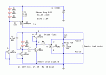
My recommendation would be the Salas v1.0 shunt regulator.
Tom, that sure is a lot of in-depth work. I hope Kuro appreciates it.
Well, I had all of the simulation bits already configured and at hand. So I was running simulations within about ten minutes of deciding to do it. It did take "several" hours. But I did it more out of my own curiosity than anything else. However, I do hope that someone else might find it at least a little bit useful.
Cheers,
Tom
Hi Tom,
Thanks for your lengthly reply. You have given me some ideas.
I went on to search for LT1084 in the forums and found some other threads on lowering noise. Now I'm off the tangent and I want try using a precision voltage reference in place of resistor R2 in my LT1085 5V regulator circuit.
I noticed that people have been using LM329. And for 5V output, 2 green LEDs. I actually want to try 2 green LEDs as voltage reference in place for R2. However, I'm worried that the 2 LEDs may not give me the 3.9V reference voltage as desired. It maybe 4V or more, which is too much.
Is there any other voltage reference I can use here in place of R2? What about adjustable voltage reference?
Hi Salas,
Off topic:
It's good to see you in here! I recall my last conversation with you was some 1-2 yrs ago with modding the Benchmark DAC1 using Auricap. Are you still using the Benchmark?
On topic:
I've heard so many good things about your shunt regulator. However, heat and space are my constraints. Currently, my LT1085 is already dissipating 5W of heat. I don't want to have more heat than what I already have. Any other suggestion?
Yes I still have it, but I am listening to vinyl only almost nowadays. I will take it to a friend's soon to compare a couple of DIY DACs with I to V, transformer and valve output, and see if I will like them better. One of those DACs has my regs all over, LV & HV.
If you could use a nice sink and burn 12W heat, that one I posted, people that used it on Buffalo in lower current, still with remote sensing, say it ousts LT and the like in a big way subjectively, even some other special discrete regs. That's the feedback I got, but I can't attest to that personally since I haven't used it on such. My suggestion would be to use a dedicated box that has a back sink so to locate it far enough and not revolve around commercial series reg chips. 4 wire Kelvin connection will make it feel in touch with its load though.
If you could use a nice sink and burn 12W heat, that one I posted, people that used it on Buffalo in lower current, still with remote sensing, say it ousts LT and the like in a big way subjectively, even some other special discrete regs. That's the feedback I got, but I can't attest to that personally since I haven't used it on such. My suggestion would be to use a dedicated box that has a back sink so to locate it far enough and not revolve around commercial series reg chips. 4 wire Kelvin connection will make it feel in touch with its load though.
- Status
- This old topic is closed. If you want to reopen this topic, contact a moderator using the "Report Post" button.
- Home
- Amplifiers
- Power Supplies
- +5V high current low noise regulator?