Hi Andrew,
I can not see any real problem moving the blue wire to the RCA's. There is no current flow in this ground connection.
I can see that as I have drawn it that it implies the two channels on one PCB, which may be better if more awkward. Even with separate PCB's however the principle is the same, "two blue wires" one to each input ground, and there is still no potential difference between them.
As to the blue wire picking up interference, maybe it isn't very susceptible to pick up as there is no "loop" for an induced current to flow.
Two separate PCB's though, yes there is a loop, so yes in that case beware.
JCX, I agree with your statement that the combined currents in the + and - supply lines will be linear and reflect the load current. However, when the amp is running class B, only one of the supply leads is carrying current (half cycle) and this is full of harmonics. I think this is what amplifer guru was referring to and trying to minimize the coupling of the garbge into the small signal stages. This is a tradeoff between minimizing the loop area or dealing with the spray harmonics.
Hi,
if only one of the supply lines is carrying that half waveform then some other wire is returning that same current back to the PSU. It must be a loop. That loop will try to generate a field. Minimise the field.
Now, back to the dual Blue Signal Ground.
If the RCAs are not commoned and there are two Signal Ground wires then the loop between these two wires is capable of generating an EMF due to external fields. That input loop area must be minimised to minimise the EMF on the Signal Grounds.
The smallest loop area will be a single wire and that demands a commoned pair of RCAs.
I have just looked again at D.Self's ed2 grounding scheme. It shows the Signal Ground going from RCA through the input screen (missing/bypassing the PCB) then connected to the Audio Ground. Except for using the screen this is topologically the same as Leach's alternative. What is missing from the ed2 diagram are the power ground and Zobel return and PCB Signal Ground connections to the Audio ground. I like to see these as separately connected to Audio Ground. Many PCB designers combine them into one return wire.
Comments?
Finally I seem to have made some sense of all this. I have been speaking to AndrewT over the grounding scheme of DSelfs amp and we are both in agreement that the official PCB layout and proposed wiring layout certainly appears incorrect.
This has caused me much confusion over the years, I felt it was "inconsistent" to say the least with all that Doug had said on layout etc at the time.
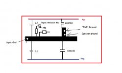
Even as a Monoblock it's not ideal. There are two 0.1 mfd caps that feed into the input ground carrying rail disturbances into the critical input ground.
Having built these amps some 14 years ago I yesterday modified the boards. Cutting the input ground, this point was now directly returned to the star. Also the speaker return was taken off the PCB and returned to the star. For the first time the amp was now silent, no audible hum/buzz etc. All the hours I spent on this at the time as well. The problem of the channel interaction that was again a major puzzle disappeared.
This diagram shows the grounding of the original PCB with the main components laid out as they actually appear.
This has caused me much confusion over the years, I felt it was "inconsistent" to say the least with all that Doug had said on layout etc at the time.
Even as a Monoblock it's not ideal. There are two 0.1 mfd caps that feed into the input ground carrying rail disturbances into the critical input ground.
Having built these amps some 14 years ago I yesterday modified the boards. Cutting the input ground, this point was now directly returned to the star. Also the speaker return was taken off the PCB and returned to the star. For the first time the amp was now silent, no audible hum/buzz etc. All the hours I spent on this at the time as well. The problem of the channel interaction that was again a major puzzle disappeared.
This diagram shows the grounding of the original PCB with the main components laid out as they actually appear.
Attachments
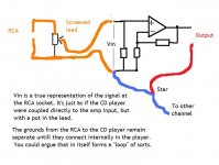
I feel the best solution may well be to have the left and right channels on a common PCB. Even with the above diagram can we really say the volt drops caused by the input circuit wiring ie the music signal from the player causing a volt drop in the wiring is zero. In the pursuit of perfection probably not.
Also the now separate grounds from input, back via the pot, then via the cables to the CD player also form a loop of a sorts.
Certainly worth thinking about !
Ultimately I have been pleased to not only find an answer after all these years, but to have increased my understanding of this subject.
Karl
Mooly said:I feel the best solution may well be to have the left and right channels on a common PCB. Even with the above diagram can we really say the volt drops caused by the input circuit wiring ie the music signal from the player causing a volt drop in the wiring is zero. In the pursuit of perfection probably not.
Also the now separate grounds from input, back via the pot, then via the cables to the CD player also form a loop of a sorts.
Certainly worth thinking about !
Ultimately I have been pleased to not only find an answer after all these years, but to have increased my understanding of this subject.
Karl
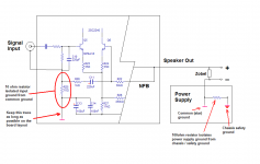
Your diagram in post 45 looks good to me.
Loops are not important unless the current flow around them causes enough voltage drop to be significant.
I'd recommend keeping the two channels gnds together as far as practical and minimizing the loop area where they are split. You can connect the RCA connectors gnds together at the case panel. Avoid allowing the RCAs to gnd to the case itself at this point - use insulators.
Glad you've banished the buzzing.
What you have drawn is a facsimile of Fig 14.1 "Grounding scheme for a typical power amplifier"from Douglas Self's book. 3rd Edition.
The only thing missing is the power transformer and main power supply caps.
What you have noted in respect to moving the grounding point for the 0.1uF caps is what D Self referred to as Distortion number 5: rail decoupling distortion (see Chapter 6). Moving the grounding point of these caps to the star ground predictably provides the benefit you observed.
With regard to reducing the Class B related noise currents in the power supply lines, this was first published by Cherry in 1981. The AES paper is worth digging out as it makes more sense than Self's writing on the topic as I recall.
I am not surprised by the confusion over a suitable remedy. Self describes two solutions with no preference given.
1. tightly twisting + and - and GND wires
2. tightly twisting just + and - wires.
More relevant is his advice to reduce the loop area in the input and feedback circuits of the amplifier. This is standard designing for EMC advice familiar to most engineers.
VivaVee said:What you have drawn is a facsimile of Fig 14.1 "Grounding scheme for a typical power amplifier"from Douglas Self's book. 3rd Edition.
The only thing missing is the power transformer and main power supply caps.
What you have noted in respect to moving the grounding point for the 0.1uF caps is what D Self referred to as Distortion number 5: rail decoupling distortion (see Chapter 6). Moving the grounding point of these caps to the star ground predictably provides the benefit you observed.
With regard to reducing the Class B related noise currents in the power supply lines, this was first published by Cherry in 1981. The AES paper is worth digging out as it makes more sense than Self's writing on the topic as I recall.
I am not surprised by the confusion over a suitable remedy. Self describes two solutions with no preference given.
1. tightly twisting + and - and GND wires
2. tightly twisting just + and - wires.
More relevant is his advice to reduce the loop area in the input and feedback circuits of the amplifier. This is standard designing for EMC advice familiar to most engineers.
Hi Vivavee,
I built these amps on the PCB's supplied by the magazine at the time. The PCB's approved by Doug do actually have the caps in a position that will introduce his distortion number 5 as I have shown into the input ground.
I have all the copies of the original articles and Doug was meticulous in his reasoning.
I can only say Doug must have been having a bad day when he approved the board layout and notes. Not just the cap error but the return of the speaker ground as well onto the PCB itself.
I have the construction notes supplied with the boards and
these show clearly how the problem will arise. Its a fundamental error as far as I can determine.
In all the follow ups and letters that followed the layout never got a mention.
Thanks for the interest, you don't know how much time I spent on this all those years back trying to eliminate all the noise. I knew it was wrong, but couldn't quite believe it
")
Regards Karl
 Wheres my ice cream ?
Mooly:
We have have bad days. As far as pcb design goes, sometimes it just gets too hard to tick ALL the boxes in terms of good design. Without looking at the pcb design in question, I can't really comment any further.
Destroyer X;
This discussion is about reducing clearly audible hum and noise at the output of power amplifiers. The difference is clearly audible and clearly better if the concluding advice is followed - you are up for an awful lot of coke +/- icecream!
We have have bad days
. As far as pcb design goes, sometimes it just gets too hard to tick ALL the boxes in terms of good design. Without looking at the pcb design in question, I can't really comment any further.Destroyer X;
This discussion is about reducing clearly audible hum and noise at the output of power amplifiers. The difference is clearly audible and clearly better if the concluding advice is followed - you are up for an awful lot of coke +/- icecream!
The discussion is about where to ground-tap the NFB of an un-balanced amplifier.
So, of course, not polluting the NFB's groundpoint with return AC from the speaker ground line does apply. Or there's the option of putting equal amounts of that, evenly into both inputs of the amplifier for a partial cancellation.
The two approaches do sound different.
One is cleaner.
The other is more exciting.
Listen for an hour and. . . cleaner wins.
Although I'm about the least educated member of this discussion, I think I'm understanding it. THANKS GUYS!!!
Even better, applying it is fun because differences in audio are fun, especially when it costs absolutely nothing to make a big difference.
So. . . Where's my ice cream?
The discussion of signal options got me into some extra thinking. . .
But, I'll just make this fast and give an example for testing.
2 of 330R, 1/2w (or 1w or 2w) carbon film resistors
2 of 10k, 1/4w (or 1/8w) metal film resistors
1 big op amp
A 330R 1/2w carbon is at the + input
A 330R 1/2w carbon is at the - input
A 10k 1/4w metal is used for feedback
A 10k 1/4w metal is used for input load
I cannot explain how this works.
My observation is that the technique does more than it should. A solid explanation is missing. . . Have fun!
EDIT: I posted this because its somewhat related to the Dr. Cherry mod, albeit I was more fascinated over the type of resistor (its huge) than any of the values. Lo-band (audio) does more easily pass through a large carbon resistor than hi-band. So, does this mean "more audio" less noise?
Hi,
Here is how I've been doing it lately with exceptional results. My amps are dead quiet and I haven't had a ground loop since.
Input signal ground shares an isolated area with NFB ground return. This is separated from the common star ground by a 10 ohm resistor, which discourages current flow from the common ground back into the input.
NFB is tapped off the output trace near the speaker out connection.
Zobel is off the amp board and mounted near the speaker out binding posts.
Speaker ground connection goes directly to the common star ground on the power supply.
Common star ground is isolated from the chassis / safety ground with a 100 ohm resistor.
Attachments
MJL21193,
This is what I do. I have not tried the 100 Ohm between system ground and chassis though. You use 10 Ohms, I use 22 Ohms. Like you I have a completely quiet system. I actually put a scope on the output with input shorted the other day to check. My scope has a 1mV /div resolution - I can just detect some change when I switch the scope input betwen 0V and the probe input.
I jus t wish I knew all these tricks when I built that damn
Elektor Equa amp 30 years ago!
Hi MJL21193 and Bonsai,
Very similar to the scheme I used on my Mosfet amp ( which is an integrated just to confuse things ) .
Bonsai, I know exactly what you mean. Hum, noise, buzzing, these were always the problem with home constructed stuff.
You really really really, yes really, don't know how much time I spent on those Class B amps over the years
- Status
- This old topic is closed. If you want to reopen this topic, contact a moderator using the "Report Post" button.
- Home
- Amplifiers
- Solid State
- 3 stage LIN topology - NFB tappings?