Dear Harry,
I am not an expert on minor loop feedback theory. Can you help me how to simulate this in this case?
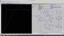
Simulation of output stage with square wave shows a small peak after start of rising edge. This peak may cause beginning of ringing due to output capacitance (= input capacitance of power bjt's)
next steps for testing:
")
BR, Toni
I am not an expert on minor loop feedback theory. Can you help me how to simulate this in this case?
Simulation of output stage with square wave shows a small peak after start of rising edge. This peak may cause beginning of ringing due to output capacitance (= input capacitance of power bjt's)
next steps for testing:
- remove the paired drivers / reduce to only one driver
- replace driver by e.g. TTC5200/TTA1943
- change base stopper resistor values
BR, Toni
Attachments
Last edited:
New Driver structure?
It seems that the two 2SC4793 TO220 drivers and complements could be replaced by a horde of faster TO126 class transistors with lower total capacitance and better total SOA.
One 2SC3503 or 2SC3601 per output perhaps?
Seems attractive to have each TO126 drive an output directly, to allow shorter traces and lower inductance.
Some one must have tried this, any references?
Best wishes
David
Last edited:
The 1R (now .47R) driver degeneration acts like a base stopper for the outputs. Combined base stopper impedance for 8 pairs with 4.7R stoppers is .59R, so with a combined driver degeneration of .5R you've doubled this. So changing to .47R decreases the base stopper phase shift significantly. The Re of the drivers at 4mA each is about 1.9R though, which would seem to swamp all of this. Maybe you should increase driver bias? Also, are the resistors used inductive?
I see two possibilities, barring inductive resistors. One is that the base stoppers add phase shift that is not agreeable to the compensation scheme. Some amps complain and others don't. The other possibility is that the resonance is caused by local parasitics and the driver degeneration plays a significant part in this.
Why don't you examine square response in LTSpice? I am currently having problems with high slewrate behavior myself. For instance, on a pulse the driver stage will go into class AB with one driver turning off, and this changes AC behavior completely during the pulse. With 8 pairs of outputs, your drivers are VERY stressed at RF. Have you tried increasing driver bias? I thought it was quite low. Also, the VAS may be turning off at negative pulses and pushing many mA on positive pulses. Both these extremes alter AC behavior dramatically.
You may try ferrite beads instead of stoppers. FB73 ferrites seem (from my limited knowledge) to be a good suggestion; LTSpice has a ferrite component. Consider that base stoppers act like output degeneration of Rstopper/Hfe.
Dear keantoken,
THX. Very good hints for further tests.
Btw doubled the driver bias on reducing R17 from 68R to 33R. Ringing betters significantly! Have to check driver SOA again, but think we are save here.
Btw. all resistors are low inductive metal film 1%.
BR, Toni
It seems that the two 2SC4793 TO220 drivers and complements could be replaced by a horde of faster TO126 class transistors with lower total capacitance and better total SOA.
One 2SC3503 or 2SC3601 per output perhaps?
Seems attractive to have each TO126 drive an output directly, to allow shorter traces and lower inductance.
Some one must have tried this, any references?
Best wishes
David
Maybe an idea for another project. But doing so stresses the VAS with higher output capacitance...
C16 should be chosen carefully. At pulse behavior, the drivers will go into class AB. When this happens the driver stage becomes a rectifier and C16 becomes the reservoir. A strong pulse will charge C16 and it will take some time for it to discharge, during which BOTH drivers will be off and the feedback loop in limbo, and until it is discharged the outputs may be biased destructively high. It is best not to use too large a cap here. You may put reverse schottkeys (1N5819) across the B-E of the drivers, which may help as a worst-case measure.
Ultimately, I wonder if having this many outputs is a liability for this kind of problem, because if your drivers are biased at the same current you'd use for 2 pairs, then for 8 pairs the discharge will be 4 times slower. To counteract this you'd need to increase driver bias by 4 times, and probably use paralleled drivers.
As far as parasitics, the output parasitics are reflected through the driver Hfe and Cbe. Using faster drivers will only work to a point. Since the outputs are the slowest and most limiting part of the amp, I see the most potential in upgrading them first. I would switch to the MJLx281/x302 series which is much faster than the C5200/A1943. Faster outputs will also decrease problems associated with C16.
the MJLx281/x302 series which is much faster than the C5200/A1943.
Are they "much faster"? The C5200/A1943 data sheets I have don't include graphs of Ft vs. IC so it's hard to compare but MJL3281 quoted Ft minimum is 30 MHz @ 1A/5V whilst 2SC5200 quoted typical is identical to this. One would therefore assume that the MJL3281 is indeed faster, but perhaps not significantly so (especially on a logarithmic frequency scale).
Maybe an idea for another project. But doing so stresses the VAS with higher output capacitance...
The total capacitance of 2SC3503 times 8 is LESS than two of your drivers.
So stress should be less.
Plus faster, lower inductance and better total SOA so bias could be increased if needed.
Best wishes
David
Thanks for this Toni.positions of Lp1, 2, 3, 5, 7 & 9 are OK. But using only inductance for simulation is wrong as keantoken correctly states.
I did say the Ribbon Cable simulation was very crude. Yes. It's a transmission line but a short & misterminated one. On that basis, the added inductance is probably the most important correction to the sim. There is already alot of capacitance on the line due to the BJT models.
The 'cure's to Toni's small oscillations all seem to hinge on changing the series bits on the feed to drivers & outputs. Hence any parasitic L would affect this.
But I really wanted to see what problems were potentially introduced by the ribbon.
For what it's worth, my crude simulations show it is actually the lead between PGa & PWRGRND which is the most critical. But the model is still far from how I would like to see it.
Toni still hasn't told me how clean GND (which exists only on the small PCB) is connected to his starpoint.
I wrote my own linear Circuit Analysis package in the early 80's when I got fed up with checking the algebra on my s=jw models. I spent many hours converting early SPICE models to the format my programme could use. In dem days, I figured I could do 'linear' stuff as good as the existing SPICE cos their models were really crude.
When I started using it for Power Amp design, the 'Ah ha!' moments were always when the model was enhanced to show some 'real life' effect. One such moment was PSU lead lengths. Post #14 of stability-analysis-ef-output-stages is an example where the sim was adjusted to reflect 'real life'
Hmmm.mmm! I'm guessing but perhaps putting small (100u) electrolytics across the nearest of Toni's 0u1s to the drivers might help.
I would personally replace all the 0u1s with small electrolytics .. as I said earlier._________________
Toni, I actually saw this in my sims but figured the driver emitter resistors had to remain at 1R to avoid problems with current sharing.The ringing has significantly lowered after reduction of emitter resistors of paired drivers from 1R to 0.47R.
Actually my sims don't show the ringing on the upward slope. Only the 'oscillation' along the bottoms of the square wave. Getting rid of R35/36 or the 1R driver emitter resistors both helped this .. but I thought removing R35/36 was safer.
I never thought of just reducing them.
__________________
An even more evil situation is when the amp is overloaded.C16 should be chosen carefully. At pulse behavior, the drivers will go into class AB. When this happens the driver stage becomes a rectifier and C16 becomes the reservoir. A strong pulse will charge C16 and it will take some time for it to discharge, during which BOTH drivers will be off and the feedback loop in limbo, and until it is discharged the outputs may be biased destructively high. It is best not to use too large a cap here.
In simpler amps, eg post #4 of tpc-vs-tmc-vs-pure-cherry, the cap has little or only bad influence on THD and definitely bad influence on overload recovery. I can confirm this in 'real life' for a very similar design. But you need it on Toni's more complex design.
...
Toni still hasn't told me how clean GND (which exists only on the small PCB) is connected to his starpoint.
...
- Input/VAS SignalGND is connected to RCA connectors GND which is connected via a thick wire to star ground.
- Output stage PowerGND is connected to star ground.
- Power supply GND is connected to star ground.
- Speaker GND is connected to powersupply ground.
The 10R resistor on the simulation file near V+/V- voltage sources is only for testing and for stability safety (measurements and/or repair situations) and as stated before can be reduced to 0.001R during simulations.
Due to reduction of R17 and higher bias the simulation shows better THD without C16. After rechecking the driver SOA I will remove C16. Maybe this helps.
"Gute Nacht!"
BR, Toni
Thanks for this Toni.
- Input/VAS SignalGND is connected to RCA connectors GND which is connected via a thick wire to star ground.
If you do this, you may want to join each RCA GND to chassis via 100n ceramic with the SHORTEST POSSIBLE LEADS. Otherwise, the input shields will conduct RFI straight into the amp. You'll want to do something like this on BOTH sides of the speaker terminals too.
I'm a bit nervous about separate star grounds for each channel.Star ground exists per channel and each star ground is connected via 10R/0.1µF parallel and a 35A bridge-rectifier parallel as 70A diode/reverse diode to earth/case.
Am I right that R76 10R is on the small PCB?The 10R resistor on the simulation file near V+/V- voltage sources is only for testing and for stability safety (measurements and/or repair situations) and as stated before can be reduced to 0.001R during simulations.
_________________
After my last post, I was staring at my Jurassic 'real world' results in #14 stability-analysis-ef-output-stages and trying to remember what I'd learnt. The oscillation I saw was very like what you report on the upward slope.Due to reduction of R17 and higher bias the simulation shows better THD without C16. After rechecking the driver SOA I will remove C16. Maybe this helps.
I didn't want to try evil Ccbs so the only thing left was damping the cap between the output bases.
I was also looking for something which showed the effect of the changes we made to base & emitter resistors. I found it by looking at V(outa) as well as V(out). Most useful was square waves with different pure cap loads. 33n seems to be worst case.
There is a lot of slew limiting in these high level square waves .. just check by looking at 5.56Vp as well as 55.6Vp 100kHz squares. This is in spite of the amp having about 90V/us slew because the inherent bandwidth is nearly 1MHz.
To ensure no slew limiting and hence no TID & other wonky measures, the input bandwidth needs to be restricted to -3dB 100kHz which you can do with 10n on InP in conjunction with R60 150. You'll want to use a more sophisticated method in case you feed InP from a 10k pot. But this will do for sims.
Tests without bandwidth restriction started with 10R in series with C16 and ended up with it removed C16 completely.
On the squares into 3n3, the wriggles on the flat part of the square are minimized and no longer as level dependent.
THD with R17 68R varies only a little from C17 470n to its complete removal.
Last edited:
Very good hint. Will RCA GND connect via zobel 0.1µF/10R directly to chassis. Or better to use only 0.1µF?...
If you do this, you may want to join each RCA GND to chassis via 100n ceramic with the SHORTEST POSSIBLE LEADS. Otherwise, the input shields will conduct RFI straight into the amp. You'll want to do something like this on BOTH sides of the speaker terminals too.
removal.
...
Speaker terminals: One 0.1µF/10R zobel directly between +/- terminals and one zobel from "-"terminal directly to chassis?
Think of two complete monoblocks in one case....
I'm a bit nervous about separate star grounds for each channel.
...
Yes....
Am I right that R76 10R is on the small PCB?
Bandwidth limiting can be seen in post#1 schematic, but not correctly calculated (~ 3.9 MHz - too high). The final drawing will definitely have something like 100 - 150kHz limit (0.1µF/10R Zobels are at about 160kHz)....
There is a lot of slew limiting in these high level square waves .. just check by looking at 5.56Vp as well as 55.6Vp 100kHz squares. This is in spite of the amp having about 90V/us slew because the inherent bandwidth is nearly 1MHz.
To ensure no slew limiting and hence no TID & other wonky measures, the input bandwidth needs to be restricted to -3dB 100kHz which you can do with 10n on InP in conjunction with R60 150. You'll want to use a more sophisticated method in case you feed InP from a 10k pot. But this will do for sims.
...
Today C17 will be desoldered!...
THD with R17 68R varies only a little from C17 470n to its complete
removal.
...
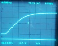
Does the slew rate limit explain the constant frequency of the ringing? A small signal square wave has the same amount of steps inbetween 1µs window as a high level square wave (see pictures from post#252 ).
Thanks so much you for helping.
BR, Toni
Toni, I actually saw this in my sims but figured the driver emitter resistors had to remain at 1R to avoid problems with current sharing.
Dear kgrlee,
do you think 0.47R driver emitter resistors are too low? Both drivers are matched to hfe + vbe.
BR, Toni
C16 removed. R17 is now 33R
C11/100n is needed otherwise higher THD.
Rising edges still have some ringing. ... back to the roots ...
Using my old development sample I decided to change base resistors of output stages ({Rb1}) from 4.7R to (empirically determined) 18R. Simulation shows a small increase of THD20k of about 0.2 ppm.
But:
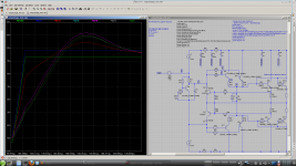
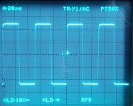
Made new square wave tests - see attached pictures. Significant better. Without load there is now a very clean rising edge and 8R load shows a small but good damped ringing. Also attached a picture of a 20kHz square wave 25V peak2peak@8R. No overshoot, no ringing.
Best performance can be achieved with TMC 68p/470p/1k to 82p/470p/1k.
Slew rate >50V/µs
The attached LTSpice file includes all of our small changes.
Again: thanks for helping.
C11/100n is needed otherwise higher THD.
Rising edges still have some ringing. ... back to the roots ...
Using my old development sample I decided to change base resistors of output stages ({Rb1}) from 4.7R to (empirically determined) 18R. Simulation shows a small increase of THD20k of about 0.2 ppm.
But:
Made new square wave tests - see attached pictures. Significant better. Without load there is now a very clean rising edge and 8R load shows a small but good damped ringing. Also attached a picture of a 20kHz square wave 25V peak2peak@8R. No overshoot, no ringing.
Best performance can be achieved with TMC 68p/470p/1k to 82p/470p/1k.
Slew rate >50V/µs
The attached LTSpice file includes all of our small changes.
Again: thanks for helping.
Attachments
Last edited:
The total capacitance of 2SC3503 times 8 is LESS than two of your drivers.
So stress should be less.
Plus faster, lower inductance and better total SOA so bias could be increased if needed.
Best wishes
David
Dear David,
nice idea to build discrete Darlingtons. To get them stable would be a challenge ...
Need to simulate this.
BR, Toni
C16 should be at least around 5 times the combined Cbe of the outputs. The time constant of C16 and R17 should be at least 5 times the max risetime expected. The Fc of 470nF*68R is 5KHz, so this demonstrates why pulse behavior with 8 output pairs could be a problem when using a driver stage not adequately scaled from a smaller amp.
astx, BJT degeneration for thermal protection depends on the thermal feedback of the transistor in question, which itself depends on the dissipation, thermal resistance and Iq. Thermal feedback has to be lowered enough by degeneration. Thermal gain must be no more than 1 for there to be thermal stability. So how do we understand thermal gain?
Thermal gain is caused by a transistor's positive dissipation tempco, which is a combination of its Vq, Vbe tempco and Rm. A 2SC5171 biased at 10mA at 40V has an Rm of 2.7R and a dissipation tempco of 2.2mV/2.7R*40V=32.6mW/C, where 2.2mV is the Vbe tempco. Without a heatsink, Rtja for this transistor is 75R. 32.6mW*75R=2.445C, so thermal gain is 2.445C - unstable. Now we need to solve the equations to know the minimum Rm necessary for thermal stability. For a thermal gain below one, our dissipation tempco needs to be less than that of Rtja. 1C/Rtja=13.3mW/C. 2.2mV/(13.3mW/40)=6.62R. Our Rm must be at least 6.62R for a bare 2SC5171 to be thermally stable at 10mA*40V. So the minimum degeneration is 3.92R IF you're not using a heatsink. With heatsink, thermal gain is no more than 10 times less (Rtjc is 7.5R, by the datasheet). So it seems full differential stability MAY be possible without degeneration IF you use a heatsink AND/OR thermally couple the drivers.
Lets apply this to your output stage. Say your setup has a total Rtja of 2R. Outputs biased at 57mA for proper null point at 71V. 1C/2R=500mW/C. 2.2mV/(500mW*71V)=.31R. So our Rm must be at least .31R. With .47R emitter resistors, combined Rm for one of your outputs is .94R, so your thermal gain is about 1/3rd. It's stable, assuming Rtja really is somewhere around 2R.
This needs some context. Since you use 8 outputs on the same heatsink, their combined thermal gain will be 8 times as much. To make this stage thermally stable without a Vbe multiplier (which directly cancels thermal gain), you would need enormous emitter resistors.
On an individual level to each output, it still applies. Two paralleled outputs will have a differential thermal gain. For this reason if differentially unstable (even if globally stable), one output will rise in bias and the other will decrease. Because the differential Vbe tempcos as well as degenerations add, the total differential gain is the same for any number of paralleled outputs. So if a single pair of outputs is thermally stable, then any number of paralleled outputs will have an even greater differential stability because the resistance between them individually will be lower than Rtja.
Last edited:
Dear keantoken,
Thank you for answer. Many new things to learn. Have had to read it minimum 10 times.
You say not to remove C16 but make it
About thermal section: maybe you can do such a really important calculation also for the currently used 2SC4793/2SA1837? Thanks in advance.
BR, Toni
Thank you for answer. Many new things to learn. Have had to read it minimum 10 times.
C16 should be at least around 5 times the combined Cbe of the outputs. The time constant of C16 and R17 should be at least 5 times the max risetime expected. The Fc of 470nF*68R is 5KHz, so this demonstrates why pulse behavior with 8 output pairs could be a problem when using a driver stage not adequately scaled from a smaller amp.
You say not to remove C16 but make it
5 * ( (8*Cbe_of_TTC5200) + (8 *Cbe_of_TTA1943)).
Where to find such knowledge as a DIY? Aaahh: Cbe is also missing from datasheet...
About thermal section: maybe you can do such a really important calculation also for the currently used 2SC4793/2SA1837? Thanks in advance.
BR, Toni
Dear David,
nice idea to build discrete Darlingtons. To get them stable would be a challenge ...
Need to simulate this.
BR, Toni
Here we are ...
Something to play with - untested! 5minute sim! Not for production!
Attachments
astx, you are basically correct on my ideas for C16. The problem is this will probably make it enormous and without a proportional increase in driver bias, you may run into bias pumping on square waves which can destroy the OPS. Best to simulate before testing.
Because the 2SC4793/A1837 appear to have the same thermal resistance as the C5171/A1930, and that the Rm of all BJTs is very similar, the same estimations apply. There are cases, such as input stages where base source impedance is several Kohms, that Ib tempco needs to be added to the calculation.
Because the 2SC4793/A1837 appear to have the same thermal resistance as the C5171/A1930, and that the Rm of all BJTs is very similar, the same estimations apply. There are cases, such as input stages where base source impedance is several Kohms, that Ib tempco needs to be added to the calculation.
- Home
- Amplifiers
- Solid State
- 2stageEF high performance class AB power amp / 200W8R / 400W4R