Have simulated outputstage performance:
THD1k@200W@8R: 0.011435%
THD20k@200W@8R: 0.022590%
THD100k@200W@8R: 0.133193%
Not so bad as we have no global feedback.
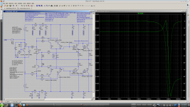
At about 5.5MHz there is a peak. Could that be the reason of the square wave instability which must be addressed by stronger compensation?
BR, Toni
THD1k@200W@8R: 0.011435%
THD20k@200W@8R: 0.022590%
THD100k@200W@8R: 0.133193%
Not so bad as we have no global feedback.
At about 5.5MHz there is a peak. Could that be the reason of the square wave instability which must be addressed by stronger compensation?
BR, Toni
Attachments
...
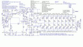
Note that the VAS is on the same rail as the positive drivers, but not the negative drivers.
...
VAS+ is double decoupled from V+
VAS- is double decoupled from V-

You can get rid of the peak by shorting out R35/36, the 68R feeds from the Bias Q8.Have simulated outputstage performance:
THD1k@200W@8R: 0.011435%
THD20k@200W@8R: 0.022590%
THD100k@200W@8R: 0.133193%
Not so bad as we have no global feedback.
At about 5.5MHz there is a peak. Could that be the reason of the square wave instability which must be addressed by stronger compensation?
This also gets rid of the small wriggles for high level square wave sim that you report in #233.
But the ribbon cable is a major factor in this. I don't think this is an accurate sim. but it may be worth trying on the real life Cherry version.
I must stop doing little bodge sims and find time to do this properly.
This is why I recommended replacing the zillion 0u1s with electrolytics. Electrolytics have just the right amount of series resistance to damp the line. They have to be AT the devices.keantoken said:Note that the VAS is on the same rail as the positive drivers, but not the negative drivers. Thus the VAS current for the negative drivers travels in a larger loop and through two sets of decoupling. This loop can be shorted by placing decoupling across the rails at the driver collectors.
This is all stuff to keep in mind and to try, to see if there is an effect, although it may do nothing. Note that introducing high-Q decoupling just anywhere will create troublesome resonances, so it is helpful to have some tiny lossy lytics on the rails (.2R-1R) for effective dampening.
It may do nothing but it certainly affects stability & THD when you try more complex compensation.
Last edited:
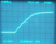
Using this .ASC, the Square Wave still shows slight overshoot .. exactly like #235. Are the BJT models the same as in #214?from #237 ... Maybe you have rise/fall time set to zero which smoothes your square wave. LTSpice seems to not accept zero here and replaces rise time by a programming default. I always set rise/fall time to 1n and 10n to see what happens.
Attached my asc file.
I can see the small wriggles in both my #235 model as well as yours from #237. As I said, shorting out R35/36 'cures' this but I'm suspicious of the simulation cos the ribbon cable.
Last edited:
Using this .ASC, the Square Wave still shows slight overshoot .. exactly like #235. Are the BJT models the same as in #214?
I can see the small wriggles in both my #235 model as well as yours from #237. As I said, shorting out R35/36 'cures' this but I'm suspicious of the simulation cos the ribbon cable.
No change of bjt models. I have also used directly your latest simulation files to test. The ribbon cable has no influence. I have tested 2 versions: 1,5 inch and 10 inch long (both are AWG 18 cables). All measurements exactly the same. Square wave exactly the same. Distortion exactly the same. Would the ribbon cable be a source of oscillation there must be a significant change in frequency on using different lengths. I think we can ignore the ribbon cable.
Removing R35/36 betters the ringing after the falling edge significantly using simulation file from post #237 but a little ringing is still viewable.
Have now to remove R35/36. Both driver bjt's will get 47R base stopper resistors. Hopefully this will help stabilizing the amp.
BR, Toni
Ribbon sims?
Toni, I know you said the ribbon doesn't matter but please indulge me.
I'm including both a .ASC and a pic of my SPICE model that very crudely sims. the ribbon.
Its done with {L} for Lp1, 2, 3, 5, 7 & 9. Lp2 is 1/5 the others cos there are 5 leads in parallel. I'm assuming 20nH/inch. If anyone knows a better, simpler method, please post it.
I just want to know if Lp1, 2, 3, 5, 7 & 9 are in the right place.
I've also moved R76 to the input as its on the small PCB and created a 'PGa' node which is 'POWERGND' on the small PCB.
Is there another connection of 'clean' GND (only exists on the small PCB) to the star-point, eg via the input lead and perhaps chassis?
Attachments
As I recall the signal lines are separated by grounded lines in the ribbon, which would allow canceling of inductance like a ground plane. Thus the ribbon will behave like a transmission line with a characteristic impedance. It is possibly worth simulation capacitances as well.
astx, the VAS is non-complimentary. The positive side is the active part and it drives both positive and negative drivers. Both positive and negative driver current loops flow through the active part of the VAS. The CCS is another load on the VAS.
I wonder if you are puzzling about now on just what we are trying to do. Is there an aspect of the amp that you are not satisfied with or that you want to improve? Without an aim we can't concentrate, and progress will be sporadic and full of regressions. BW and slew rate are things you can still measure, so can be more than hypothetical.
astx, the VAS is non-complimentary.
You mean non-complemetary?
Is that like a cemetary?
I guess the word we're looking for is complementary? IE not dinner mints?
Sorry I lost one n.
Dear kgrlee, keantoken,
positions of Lp1, 2, 3, 5, 7 & 9 are OK. But using only inductance for simulation is wrong as keantoken correctly states.
About development:
The most annoying problem already exists. The 5Mhz ringing on rising edge. This frequency is constant on using 1.5 inch or 10 inch ribbon cable. As there was a 5 Mhz peak in output stage simulation and kgrlee has identified R35/36 as source I will remove this today - perhaps this will stop the ringing and we can continue with finetuning the amplifier layout.
BR, Toni
Dear keantoken, kgrlee,
maybe I found a hint what is the reason for the ringing on rising edge:
http://www.altera.com/literature/an/AN476.pdf
Page 12 / Figure 10 show square wave transients on different lengths of transmission lines. I think the ribbon cable AND the long PCB can be seen as transmission line (parallel wired and grounded).
It is now clear that the length of the cable/pcb has influence mostly on time delay which in our case may be ignored. This also explains why different lengths of the ribbon cable showed no significance difference between the measurements.
Now let's have a look on figure 11/page 13. The ringing on the rising edge is caused by output capacitance on the other side of the transmission line. If we compare the attached pictures we can see, that the ringing frequency is independend from load and amplifier output level.
I think this special type of ringing is no sign of bad phase/gain margin and no sign of amplifier instability. In real life we would never amplify a signal with a rise time of < 10ns from 10 to 90% due to limited input frequency.
Don't know how to simulate and verify this theory. Any Ideas?
On the other hand if we could savely ignore this type of ringing we can further optimize the compensation and get THD20k@200W@8R at or near 0.001%
BR, Toni
Attachments
If it doesn't respond to changes in the amp, then it must be a peripheral resonance. A CCS might be resonating, or one of your 100nF rail decoupling.
Glen Kleinschmidt has made some measurements on decoupling resonances. The smaller the film cap, the worse. 470nF and up across a low-ESR lytic begins to improve. 100nF decoupling is guaranteed to resonate. Even 1uF resonates, so it is good to put a lossy lytic, or RC damper across the film cap (.2-2R).
Glen Kleinschmidt has made some measurements on decoupling resonances. The smaller the film cap, the worse. 470nF and up across a low-ESR lytic begins to improve. 100nF decoupling is guaranteed to resonate. Even 1uF resonates, so it is good to put a lossy lytic, or RC damper across the film cap (.2-2R).
Glen Kleinschmidt has made some measurements on decoupling resonances. The smaller the film cap, the worse. 470nF and up across a low-ESR lytic begins to improve. 100nF decoupling is guaranteed to resonate.
That would depend upon the parasitic inductance and the ESR in the circuit. These in turn depend upon the terminal pitch of the two capacitors, the inductance of the board traces, and the ESR of the caps. You therefore cannot say that 100 nF is guaranteed to resonate.
If the board traces are running over a ground plane, it's fairly straightforward to accurately predict the inductance.
Anyway, I suspect that astx is correct with his transmission line theory: no change would have been observed with change of length of the ribbon cable as its characteristic impedance is independent of length.
Transmission line effects only matter at frequencies over that of the cable's wavelength. Below that it acts like an inductor and capacitor. If the circuit operating frequency is within that of the wavelength of the cable, then characteristic impedance still wouldn't matter because unless terminated properly, the standing waves (modal resonances) are a roll of the dice as to where they fall within the AC response of the feedback loop.
I think the wavelength of the cable must be shorter than any wavelengths posing a threat to the feedback loop, so what's left is the total capacitance and inductance of the cable, which does vary with length and interacts with the rest of the circuit just like any other parasitics, regardless of characteristic impedance.
While astx has shown there is no noticeable effect, I think the parasitics of the cable are just like any other parasitics present in layout, and don't earn special status because of transmission line behavior. In this case, probably due to astx's smart pairing with ground lines, they appear to be inconsequential.
I think the wavelength of the cable must be shorter than any wavelengths posing a threat to the feedback loop.
Yes.
astx is trying to amplify a square wave. Don't forget that the frequency content of the rising and falling edges of such stretch into the territory where the ribbon cable is behaving as a transmission line. Transmission line effects can then produce the staggered waveform seen on the rising edges, and the "frequency" of these ripples are well beyond the ULGF so the global feedback loop is powerless to correct them.
It's possible that as astx supposes, that it's nothing to worry about.
Perhaps this information helps us:
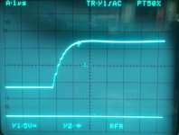
After many hours of comparing output stages with scope etc. the source of ringing seems to be introduced between base of paired drivers Q11/Q12 (Q17/Q23) and output to base of power transistors. Output capacitance load?!
The ringing has significantly lowered after reduction of emitter resistors of paired drivers from 1R to 0.47R.
All other changes like removing R35/36 have brought us little to no bettering of ringing.
Any ideas?

I've lost track: have you actually verified in simulation that the minor loop has sufficient gain and phase margins?
As you say it's usually pretty hard to determine where exactly oscillation originates because once it starts it will propagate around the loop and essentially be everywhere. Tracking down the source would normally require temporary replacement of parts of the circuit (e.g. replacement of output stage transistors with much higher-speed but much lower power capability BC5xx devices) on a trial-and-error basis.
As you say it's usually pretty hard to determine where exactly oscillation originates because once it starts it will propagate around the loop and essentially be everywhere. Tracking down the source would normally require temporary replacement of parts of the circuit (e.g. replacement of output stage transistors with much higher-speed but much lower power capability BC5xx devices) on a trial-and-error basis.
The 1R (now .47R) driver degeneration acts like a base stopper for the outputs. Combined base stopper impedance for 8 pairs with 4.7R stoppers is .59R, so with a combined driver degeneration of .5R you've doubled this. So changing to .47R decreases the base stopper phase shift significantly. The Re of the drivers at 4mA each is about 1.9R though, which would seem to swamp all of this. Maybe you should increase driver bias? Also, are the resistors used inductive?
I see two possibilities, barring inductive resistors. One is that the base stoppers add phase shift that is not agreeable to the compensation scheme. Some amps complain and others don't. The other possibility is that the resonance is caused by local parasitics and the driver degeneration plays a significant part in this.
Why don't you examine square response in LTSpice? I am currently having problems with high slewrate behavior myself. For instance, on a pulse the driver stage will go into class AB with one driver turning off, and this changes AC behavior completely during the pulse. With 8 pairs of outputs, your drivers are VERY stressed at RF. Have you tried increasing driver bias? I thought it was quite low. Also, the VAS may be turning off at negative pulses and pushing many mA on positive pulses. Both these extremes alter AC behavior dramatically.
You may try ferrite beads instead of stoppers. FB73 ferrites seem (from my limited knowledge) to be a good suggestion; LTSpice has a ferrite component. Consider that base stoppers act like output degeneration of Rstopper/Hfe.
- Home
- Amplifiers
- Solid State
- 2stageEF high performance class AB power amp / 200W8R / 400W4R