what branded output power mosfet are prefered?
Vishay.
Very intersting proposal!This is SSR (Solid State Relay) I am going to use in all my amps as loudspeaker protection. It uses Si8752 Silicon Lab isolated FET driver.
Damir
When do you plan to propose it somehow?
How fast is it?
Does introduce any distortion?
Thanks
Very intersting proposal!
When do you plan to propose it somehow?
How fast is it?
Does introduce any distortion?
Thanks
How fast it is is defined by DC offset detector and that has to recognize DC offset and that time is much longer then the SSR reaction time (that you can see in its data sheet)
Distortion should be much lover then any amp distortion and depends of the mosfets used.
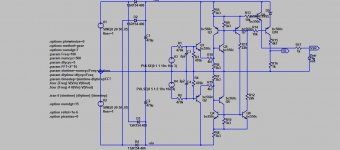
Attached schematic is of the DC offset detector and the LED and SSR mark is where the Si8752 is connected.
Attachments
I tried to test the circuit withHow fast it is is defined by DC offset detector and that has to recognize DC offset and that time is much longer then the SSR reaction time (that you can see in its data sheet)
Distortion should be much lover then any amp distortion and depends of the mosfets used.
Attached schematic is of the DC offset detector and the LED and SSR mark is where the Si8752 is connected.
An externally hosted image should be here but it was not working when we last tested it.
It has a simple way to unbalance the output.
The result is very promising:
An externally hosted image should be here but it was not working when we last tested it.
To get this result I had to modify the value of R1 and R2 to 100k. I hope that this will not lead to instabilities and that the 42ms of reaction time is short enough to save the woofers.
Anyway the behavior seems a lot better than the one I had (on the simulator) with the loudspeaker protection embedded in your MOS/BJT PSU.
let me guess that the circuit is complemented by
An externally hosted image should be here but it was not working when we last tested it.
By the way I'm stopped by SARS-COV-19: I wanted to order the PCB of the MOS/BJT PSU from JlcPCB, but now they don't deliver to Italy.
So, what do you plan to do: provide the gerber? sell the PCB's? and when?
Thanks
If you choose to low value for R1 and R2 it could be triggered with to low DC offset. R1 on that circuit is included in the SSR schematic already.
I am stopped by cov-19 too, no plans for now, probably I'll sell the pcb.
BR Damir
Waiting for the end of the pandemicI am stopped by cov-19 too, no plans for now, probably I'll sell the pcb.
BR Damir
") and for your PCB's.
and for your PCB's.Many thanks
I have checked your circuit with some real music and it appears to be very stable even if I reduce R1=R2=33k (so it becomes very fast).
However in this way the initial "anti-bump" delay is reduced.
How can I control this delay?
Thanks
If you want to have SSR delay at turn on you can delay it's power supply.
I don't have any "bump" in my amps as I used PS regulators with slow voltage build on.
Hi Dadod,
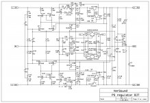
I got a chance to populate the voltage regulator this week. I powered up today with a +/- 56Vdc power supply. I installed 1A fuse on the +/- input of the regulator. After turning on the switch, Q9 went up smoke/fried. Fuse on the rail (1A) didn't blew up but the fuse on the AC input. No load was connected to the regulator, Q7 and Q107 not installed.
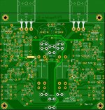
I checked the resistor values, placement and transistors on the board, So far, I didn't see anything wrong. But I noticed something on the PCB though, the two terminal of P1 is shorted but on the schematic, there's supposed to be a 22K resistor in between and labeled R126? And R123 68K across the P1. Do you think this is the problem? Attached is the regulator board. Can you check if theres something I missed or installed incorrectly?
Thanks.
I got a chance to populate the voltage regulator this week. I powered up today with a +/- 56Vdc power supply. I installed 1A fuse on the +/- input of the regulator. After turning on the switch, Q9 went up smoke/fried. Fuse on the rail (1A) didn't blew up but the fuse on the AC input. No load was connected to the regulator, Q7 and Q107 not installed.
I checked the resistor values, placement and transistors on the board, So far, I didn't see anything wrong. But I noticed something on the PCB though, the two terminal of P1 is shorted but on the schematic, there's supposed to be a 22K resistor in between and labeled R126? And R123 68K across the P1. Do you think this is the problem? Attached is the regulator board. Can you check if theres something I missed or installed incorrectly?
Thanks.
Attachments
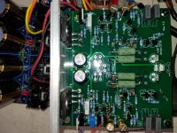
I think the problem was R23, its supposed to be 20K and I installed 68K, R123 is 68K. The resistor numbering on the schematic is a bit confusing. The resistor on the middle of P1 is still a mystery to me and no placement for 22K. Did you remove it on this version of the board and no longer necessary?
Hi Dadod,
I got a chance to populate the voltage regulator this week. I powered up today with a +/- 56Vdc power supply. I installed 1A fuse on the +/- input of the regulator. After turning on the switch, Q9 went up smoke/fried. Fuse on the rail (1A) didn't blew up but the fuse on the AC input. No load was connected to the regulator, Q7 and Q107 not installed.
I checked the resistor values, placement and transistors on the board, So far, I didn't see anything wrong. But I noticed something on the PCB though, the two terminal of P1 is shorted but on the schematic, there's supposed to be a 22K resistor in between and labeled R126? And R123 68K across the P1. Do you think this is the problem? Attached is the regulator board. Can you check if theres something I missed or installed incorrectly?
Thanks.
Hi Fred,
Sorry for this.
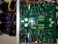
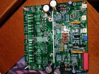
There is short between top and bottom layers showed in attached photos.
Just use some sharp knife or fast grinder and remove small part of the top layer where R1 showed in the photos.
R126 is just short connection, schematic and BOM are wrong in that part.
Check D5, probably shorted too.
Best wishes, Damir
Attachments
Thank you for your quick response. On my spare unpopulated Regulator board, I found the trace are shorted too. So means to say, its factory defect. I'm surprise that nobody made a comment about it which most of the guys is probably done with this project. Unless, they're not using the regulator. Just got the chance to work on this project because of Covid 19 situation.
Dadod, you said schematic and BOM are wrong in that part. Can you please update and gives us the latest one before I replace those bad parts and power up again .Thanks and appreciate your help.
Dadod, you said schematic and BOM are wrong in that part. Can you please update and gives us the latest one before I replace those bad parts and power up again .Thanks and appreciate your help.
Thank you for your quick response. On my spare unpopulated Regulator board, I found the trace are shorted too. So means to say, its factory defect. I'm surprise that nobody made a comment about it which most of the guys is probably done with this project. Unless, they're not using the regulator. Just got the chance to work on this project because of Covid 19 situation.
Dadod, you said schematic and BOM are wrong in that part. Can you please update and gives us the latest one before I replace those bad parts and power up again .Thanks and appreciate your help.
Corrected schematic and BOM.
Attachments
I cut the shorted trace on the PCB, replaced Q9 and R23. Powered up the regulator and no white smoke encountered. What is the minimum DC voltage or offset voltage from amp to trigger the regulator to off? Is it 1Vdc at least? I haven't tried yet but maybe next week.
Next is to start populating the amp,board.
Thank you Damir for updating the schematic and BOM.
What is the minimum DC voltage or offset voltage from amp to trigger the regulator to off? Is it 1Vdc at least? I haven't tried yet but maybe next week. Next is to start populating the amp,board.
Thank you Damir for updating the schematic and BOM.
I cut the shorted trace on the PCB, replaced Q9 and R23. Powered up the regulator and no white smoke encountered.
Next is to start populating the amp,board.
Thank you Damir for updating the schematic and BOM.
I took the idea of this DC offset detector from JLH and his power supply for 80W mosfet amp.
With the value as on the schematic the trigger DC offset value is about 6V, but there is a time constant to no to be triggered with short pulses.
If you think this is to high you can change R18, R118 (R19, R119) from 1Meg to 470k and then DC offset triger value will be a bit below 4V. I will not go lower than that.
Hi Dadod, hope doing great. I got a chance to work on my DIY stuff today. Checked the power supply regulator again and its output voltage was +/-52.8 Vdc. The unregulated input is +/-57.6 Vdc. I was expecting that it should still maintain to +/-50 Vdc output, even though the input will go up 2Vdc higher?
I also started populating the amp board but I just realize that I was not able to buy BC560 because its no longer available. Can I use BC557? It seems like the specs are the same except the (NF) Noise figure. Also, use KSA992 and KSC1845 in replacement of 2SA970 and 2SC2240. Your Amp parts are getting obsolete. Hope these replacement parts still works.
Getting ready to power up and check voltages on R5 and R6.
Attachments
Last edited:
- Home
- Amplifiers
- Solid State
- 200W MOSFET CFA amp