Something amaze-me. The disproportion between the active parts and the means to cool it.
It's High-End (with capital's)
")
Hello ATX,
With regards to "Damirs 200W CFA", I may have missed this mentioned elswhere in this thread but who designed the layout of this amplifier. Secondly is the layout of RNMarsh's amplifier the same as this layout.
Is there a link to this PCB layout , is this pcb more than 2 layers.
With regards to "Damirs 200W CFA", I may have missed this mentioned elswhere in this thread but who designed the layout of this amplifier. Secondly is the layout of RNMarsh's amplifier the same as this layout.
Is there a link to this PCB layout , is this pcb more than 2 layers.
Hello ATX,
With regards to "Damirs 200W CFA", I may have missed this mentioned elswhere in this thread but who designed the layout of this amplifier. Secondly is the layout of RNMarsh's amplifier the same as this layout.
Is there a link to this PCB layout , is this pcb more than 2 layers.
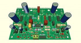
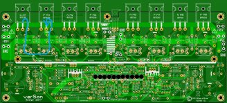
I designed it, 2 layers. http://www.diyaudio.com/forums/solid-state/243481-200w-mosfet-cfa-amp-113.html#post5277626
Damir
May-be time to reconsider the way we cool our active devices in the Hifi world.It's High-End (with capital's)
Water cooling ?
May-be time to reconsider the way we cool our active devices in the Hifi world.
Water cooling ?
Yes and no
The guy in the picture put wheels to move it.
Warning his will break you in many ways
Of with the wedding ring for safety when assembling!
Intense working out with heavy weights a key parameter in design when ready.
I love this "Viking"heavy bodybuilding,strongmans Power AMP "theme"
Something amaze-me. The disproportion between the active parts and the means to cool it.
what makes it disproportionate? The heat vs size ?
THx-RNMarsh
Its in your construction wiring layout and grounding system. Not the circuitry. Both internally and/or the testing setup.
SR is without the input RC filter.
You are comparing THD+N to my THD. (But I have both numbers and you are are still a bit higher, over-all. So, its your wiring/grounding needs improving).
THx-RNMarsh
I reply to Richards answer in this thread:
The CFA has been measured on the bench with exactly the same procedures and optimized wiring as my VFA variants. I'm sure there was no "wiring layout" problem.
You show measurements without any remark about the conditions where they have been taken. E.g. removed input filter, supply voltage, BIAS current? We only can compare measurements if we have the same start conditions. I measure always at output on speaker terminal - this is what the user hears. When I remove input filter, measure before output zobel, remove VAS diode, remove overcurrent protection then an example amplifier performs 0.001% THD+N 20k@200W@8R but this is not what the user gets ...
IMHO: THD+N and especially IMD is an indicator how good an amplifier performs. An amplifier may have good THD values at 20k full power but produces higher noise in the audio range and/or may have a not so good IMD figure.
Best regards, Toni
Hi Toni,
I’ll try to answer some of your points.
1. Input LP filter does not provoke slaw SR distortion just amplitude (linear distortion), but an amp SR could provoke TIM and PIM if not high enough.
In this case it is not really important 200V/usec or 400V/usec but real amp SR is without input LP filter and should be measured without it.
2. VAS diode? It was my old trial (failed no thermal stable) and I hope you did not measured with it. Last version uses 470uF in series with 22R paralleled to VAS emitter resistor.
3. The last PCB layout is improved to the best of my knowledge (I am not PCB layout expert just hobbyist) specially part around OPS to lower influence of high current to the around circuitry (according Cherry suggestion), you can look at last layout. In my opinion it’s very important to have as short as possible the Feed Back path specially when ULGF is high. In my amps it is between 3 and 5 MHz.
As I don’t have direct information from Bangkok I can’t comment on other things as external wiring or where the output coils are situated. The PCB has direct output too before the coil and I suggested to put the coils and parallel resistor directly at the output terminals.
BR Damir
Today the boards arrived. I will send PM to those who accepted the price, I need the PayPal email address.
I have one spare stereo set of the boards for balanced input. With those boards it's possible to transform this amp from unbalanced to balanced inputs. If someone interested, please tell, it will go with one complete stereo set. This additional board is going instead small Feedback board.
mlloyd1 4 board
AVWERK 2 board
trebolo 4 boards
and Lbud4 4 boards but not confirmed
Damir
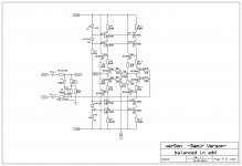
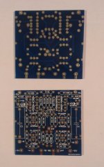
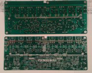
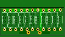
first - balanced inputs add boards schematic
second - actual balanced inputs add boards
third - main boards
forth - FB board
I have one spare stereo set of the boards for balanced input. With those boards it's possible to transform this amp from unbalanced to balanced inputs. If someone interested, please tell, it will go with one complete stereo set. This additional board is going instead small Feedback board.
mlloyd1 4 board
AVWERK 2 board
trebolo 4 boards
and Lbud4 4 boards but not confirmed
Damir
first - balanced inputs add boards schematic
second - actual balanced inputs add boards
third - main boards
forth - FB board
Attachments
Hello Damir,
Is the following link to post 1131 the actual schematic of the CFA 200W mosfet amplifier. Is this the actual final production schematic version that you built the amplifer PCBs that RNMarsh and Astx are using.
200W MOSFET CFA amp
Is the following link to post 1131 the actual schematic of the CFA 200W mosfet amplifier. Is this the actual final production schematic version that you built the amplifer PCBs that RNMarsh and Astx are using.
200W MOSFET CFA amp
Hello Damir,
Is the following link to post 1131 the actual schematic of the CFA 200W mosfet amplifier. Is this the actual final production schematic version that you built the amplifer PCBs that RNMarsh and Astx are using.
200W MOSFET CFA amp
Yes, this is last version with some minor changes compare with the boards Astx used, RNMarsh has exactly this one.
The heat ? Unless we use class D, we know we cannot do a lot better about. And class D seems not good enough, until now, to compete with the best Class AB amps.what makes it disproportionate? The heat vs size ?
It is the size, the weight and the money that seems out of proportion: Too many calories to be evacuated with passive cooling.
Last edited:
1st approach
Hi,
This is my first attempt of the CFA120 LatMos version, changing the board size to 125mmx80mm, and adapted to TO-3p output stage (transistors are mounted on an aluminum plate (150mmx80mmx10mm) under the pcb). As always i will let it rest, and have a look over it for possible improvements in the next weeks.
Maybe also start a test order of 5 PCB in China for few Euros.
Time will come and minds change sometimes
thanks dadod for this famous design
BR
Günni
Attachments
Hi,
This is my first attempt of the CFA120 LatMos version, changing the board size to 125mmx80mm, and adapted to TO-3p output stage (transistors are mounted on an aluminum plate (150mmx80mmx10mm) under the pcb). As always i will let it rest, and have a look over it for possible improvements in the next weeks.
Maybe also start a test order of 5 PCB in China for few Euros.
Time will come and minds change sometimes
thanks dadod for this famous design
BR
Günni
For input quad matched transistors you can use THAT340. I intend to use it in my next SMD PCB design.
Hello Damir,
In the final boards being measured by the guys is there over current protection not shown in the link to post 1131, that have a dramatic effect on distortion in the higher frequencies as revealed by Astx neasurements.
200W MOSFET CFA amp
In the final boards being measured by the guys is there over current protection not shown in the link to post 1131, that have a dramatic effect on distortion in the higher frequencies as revealed by Astx neasurements.
200W MOSFET CFA amp
Last edited:
Hello Damir,
In the final boards being measured by the guys is there over current protection not shown in the link to post 1131, that have a dramatic effect on distortion in the higher frequencies as revealed by Astx neasurements.
200W MOSFET CFA amp
Hello PHENIX,
There is no over current protection on any of those boards. I use voltage regulator (kind of capacitance multiplier) for my amps with over current protection and DC offset loudspeaker protection showed in this thread too.
BR Damir
Hello Damir ,
Just about the PCB did you use any special layout on the output stage to minimize the non linear magnetic field caused by the half wave current of the class A/B output stage . I dont think I see any special precautions to minimise these problems.
Hello PHENIX,
I used a kind of interweaved connection of the output mosfets, one N and next one P channel and so on, not one type on one side and the other type on other side.
In this way the half wave current of the class A/B output stage is going in smaller loops and I hope les interfere with input circuitry. I would like to hear your opinion.
Attachments
Hi Toni,
I’ll try to answer some of your points.
1. Input LP filter does not provoke slaw SR distortion just amplitude (linear distortion), but an amp SR could provoke TIM and PIM if not high enough.
In this case it is not really important 200V/usec or 400V/usec but real amp SR is without input LP filter and should be measured without it.
2. VAS diode? It was my old trial (failed no thermal stable) and I hope you did not measured with it. Last version uses 470uF in series with 22R paralleled to VAS emitter resistor.
3. The last PCB layout is improved to the best of my knowledge (I am not PCB layout expert just hobbyist) specially part around OPS to lower influence of high current to the around circuitry (according Cherry suggestion), you can look at last layout. In my opinion it’s very important to have as short as possible the Feed Back path specially when ULGF is high. In my amps it is between 3 and 5 MHz.
As I don’t have direct information from Bangkok I can’t comment on other things as external wiring or where the output coils are situated. The PCB has direct output too before the coil and I suggested to put the coils and parallel resistor directly at the output terminals.
BR Damir
Dear Damir,
don't misunderstand me. I do not want to make your amp in any way looking bad. I only want to understand the measurement differences of Richard's and my tests. Unfortunately Richard doesn't always document the environment conditions during measurements (supply voltage, bias ...).
VAS diode is meant only as an example for a blameless...
A longer feedback path isn't a problem as shown in SA2014 simulation and measurements. Of course a completely changed pcb routing can have some good/bad influence on distortion results. I will have a look on your older pcb variant and will compare this with Richards one (a link to Richards pcb version would be helpful).
BR, Toni
- Home
- Amplifiers
- Solid State
- 200W MOSFET CFA amp