This thread is about NMOS amplifiers, schematics for amplifier like kelvin is in thread:
http://www.diyaudio.com/forums/solid-state/164093-100w-ultimate-fidelity-amplifier-10.html
Regards
http://www.diyaudio.com/forums/solid-state/164093-100w-ultimate-fidelity-amplifier-10.html
Regards
Would you comment auto-bias circuit from post #53 ?C3 and R5 are part of a pole-zero compensation system.
The advantage of pole-zero compensation is higher open loop gain at mid-high frequencies, which translates into lower high-frequency distortion and lower output impedance, without any substantial degradation in stability. The usual rise in output impedance and distortion above 1khz in traditional amplifiers is moved upwards, it does not start until a higher frequency (may be as high as 20khz resulting in flat THD and constant damping factor, which makes the amplifier closer to "ideal").
Pole-zero compensation is rarely used in DIY amplifiers because it's a bit more complex than the traditional dominant pole compensation and harder to implement for people with no knowledge about feedback control loop theory (or even without an oscilloscope).
Regards
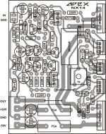
Picture is high quality, use full screen when increase picture (click on four arows down in left corner).I should study it further because at first glance I don't see how it works. There are some node names on the schematic that are very hard to read, so I don't know where are the signals coming from. A higher quality picture or pdf would help.
Regards
Last edited:
Bias is controlled through pulse width modulation.
The current flowing through the lower MOSFET is compared against a reference, which is desired bias level. It works much in the same way as a switching amplifier.
When current is below desired bias level, pwm (logic) output is on (high), otherwise it's off (low). The PWM output is lowpass filtered with a pole in the origin (like a servo) and the resulting (nearly DC) voltage is converted into current and fed to the optocoupler, which does the level shifting and sinks a proportional current from the base of the Vbe multiplier, which results in increased output stage bias.
So the more time the current through the lower MOSFET is below the desired bias level, the more bias voltage is applied to the gates of output transistors. In other words, the circuit tries to keep the lower MOSFET always biased.
I have seen this biasing scheme before, but implemented in another way. See Visch output stage (1975):
http://www.diyaudio.com/forums/solid-state/160285-class-b-w-o-crossover-distortion-1975-a.html
Thanks, what do you think about adding more outputs in parallel and increase rail voltage to get more power with this schematics?Bias is controlled through pulse width modulation.
The current flowing through the lower MOSFET is compared against a reference, which is desired bias level. It works much in the same way as a switching amplifier.
When current is below desired bias level, pwm (logic) output is on (high), otherwise it's off (low). The PWM output is lowpass filtered with a pole in the origin (like a servo) and the resulting (nearly DC) voltage is converted into current and fed to the optocoupler, which does the level shifting and sinks a proportional current from the base of the Vbe multiplier, which results in increased output stage bias.
So the more time the current through the lower MOSFET is below the desired bias level, the more bias voltage is applied to the gates of output transistors. In other words, the circuit tries to keep the lower MOSFET always biased.
I have seen this biasing scheme before, but implemented in another way. See Visch output stage (1975):
http://www.diyaudio.com/forums/solid-state/160285-class-b-w-o-crossover-distortion-1975-a.html
Regards
Last edited:

OK, thats quite low for a FET. Lateral FETS usually need 150mA and Vertical FETS are run at 400mA. If you look at the transfer characteristics in fig 3 on the link: http://www.datasheetcatalog.org/datasheet/irf/irfp250.pdf
You can see if you ran it at 400mA there is chance of thermal runaway.
I usually run mine at approx. 35mA and dont get any crossover distortion.
It is easy to get into thermal runaway with large bias currents unless there is thermal feedback.
Put 10R resistors insteads fuses, and adjust with trimpot to get 2V on them that will be bias set to 200mA,how to set the bias value?
Regards
With single pair MOSFET output stage no need for source resistor (0R1/5W). Source resistor in +V is for overcurrent detector for protect circuit NX16). Go to thread http://www.diyaudio.com/forums/solid-state/164093-100w-ultimate-fidelity-amplifier-21.html , see posts from #200 to #210.Miles,
NX14, where is the source resistor (0R1/5W) for -V in your PCB ?
Please confirm all components and connection once again before posting.
Thank you.
Raj.
Regards
Last edited:
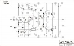
This circuit is upgrade on BUZAMP from Elektor. Use only N-mosfets, with +/-50V DC give 150W on 4R load.
Miles,
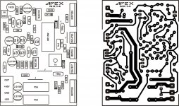
Do you have pcb layout for this?
Any other replacement for BF872?
Thanks.
NX14 is better choice for NMOS amplifier...Miles,
Do you have pcb layout for this?
Any other replacement for BF872?
Thanks.
NX14 is functional circuit, but for Hi-Fi not for PA. You can find in my other threads amps for PA.Hi Apex.....i want to build your Nx14 circuit......I have all the parts....is it a functional circuit and can I use it for my PA system.......
Regards,
Macd
Regards
- Home
- Amplifiers
- Solid State
- 150W MOSFET Amplifier with IRFP250x2