I must ask (Prof) Ed Cherry about this zigzagging tracks on pcbs - I don't recollect any details about it that Andrew indicated but he's addressing the AES meeting next month about amplifier design, so I'll ask, unless you have access to the paper in question?
Sorry, don't have access to papers
 .
.I think of this routing thing like this: when you connect board with wires with high currents, recommendation is to use twisted pair technique to minimize radiation&susceptibility to interference. So, from the same logic, pcb traces needs to try to "mimic" twisted pair configuration to achieve the same.
Does twist add something more than just "parallell" and "close"? Is twisting the best solution to keep 2 indvidual wires parallel and close?
//
Twisted pair
Twisted pair cabling is a type of wiring in which two conductors of a single circuit are twisted together for the purposes of canceling out electromagnetic interference (EMI) from external sources; for instance, electromagnetic radiation from unshielded twisted pair (UTP) cables, and crosstalk between neighboring pairs. It was invented by Alexander Graham Bell.
The close coupled parallel pair reduces loop area.
The twisted pair reduces loop area.
In that respect both are very similar.
The parallel pair always presents one of the pair to a different strength of external field.
The twisted pair swaps the wires around and presents each of the pair alternately to the different strength of external field.
In this respect paralleled and twisted are different.
The twisting has the effect of reducing emission of interference fields and reducing reception of interference fields.
The pitch of the twist affects the frequency range that the interference attenuation is effective.
Hi Sikahr,
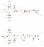
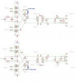
Can you show updated schematic for your PCB. I downloaded your last one and I see some extra parts like bleeder resistors and rectifier resistors which I can't find in that last schematics... I need to build dual +/0 and little confused about second +/0 like R placement for CRC on + side and jumper on - side.
Thank you.
Sent from my iPhone using Tapatalk
The close coupled parallel pair reduces loop area.
The twisted pair reduces loop area.
In that respect both are very similar.
The parallel pair always presents one of the pair to a different strength of external field.
The twisted pair swaps the wires around and presents each of the pair alternately to the different strength of external field.
In this respect paralleled and twisted are different.
The twisting has the effect of reducing emission of interference fields and reducing reception of interference fields.
The pitch of the twist affects the frequency range that the interference attenuation is effective.
Gold!
//
Hi Sikahr,
Can you show updated schematic for your PCB. I downloaded your last one and I see some extra parts like bleeder resistors and rectifier resistors which I can't find in that last schematics... I need to build dual +/0 and little confused about second +/0 like R placement for CRC on + side and jumper on - side.
Thank you.
Sent from my iPhone using Tapatalk
On vacation at the moment.
I am back Next week. Sorry.
Hi Sikahr,
Thank you, but I see something that is confusing me.
First of all, you have 2 Ele caps per rail and not 4.
C1 and C3 for "+" and C2 and C4 for "-" rail.
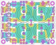
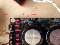
Second, (for the top positive portion of PCB) all rectifier diodes are reversed backwards on PCB silkscreen. Take a look on D1 and D3, where anode is connected to Ele cap "+", D2 and D4 cathode connected to Ele cap "-". Bottom part rectifier block has the same issue for +/GND/- configuration.
I'm going to show some corrections on your schematics (it is my point of view and may be it is absolutely wrong for others DIYers!) and pictures on my tested board. Please let me know your opinion.
Thank you, but I see something that is confusing me.
First of all, you have 2 Ele caps per rail and not 4.
C1 and C3 for "+" and C2 and C4 for "-" rail.
Second, (for the top positive portion of PCB) all rectifier diodes are reversed backwards on PCB silkscreen. Take a look on D1 and D3, where anode is connected to Ele cap "+", D2 and D4 cathode connected to Ele cap "-". Bottom part rectifier block has the same issue for +/GND/- configuration.
I'm going to show some corrections on your schematics (it is my point of view and may be it is absolutely wrong for others DIYers!) and pictures on my tested board. Please let me know your opinion.
Attachments
Hi, Alex You are right.
1. "a" caps are not real (only trick in Eagle)
2. Yup, unfortunately, all rectifier diodes have wrong polarity on silkscreen
At least, all are wrong marked
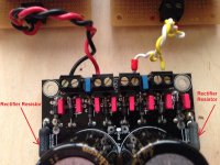
3. Rectifier resistors are correctly marked on your schematics
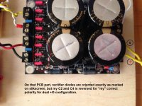
4. In your case, dual +/0, you must reverse all polarized elements on bottom block, el. caps & rect. diodes, you did this, so all is OK
BR Sika
BTW Very nice build
1. "a" caps are not real (only trick in Eagle)
2. Yup, unfortunately, all rectifier diodes have wrong polarity on silkscreen
At least, all are wrong marked
3. Rectifier resistors are correctly marked on your schematics
4. In your case, dual +/0, you must reverse all polarized elements on bottom block, el. caps & rect. diodes, you did this, so all is OK
BR Sika
BTW Very nice build
Hi Sikahr,
You are absolutely right about all point.
Also, I reversed bottom rail LED too. Sorry, I forgot to mention this.
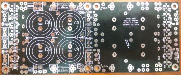
PCB itself is very nice and it is easy to work with. I surprised by Dirty PCB quality.
It is definitely decent and I see no needs to manufacture that type of PCBs in US or EU who charge x10 for the same amount ob boards.
If it is possible to change rectifiers silkscreen for Ditry PCB guys, than this board will be nice asset to any DIYer.
Thank you a lot.
You are absolutely right about all point.
Also, I reversed bottom rail LED too. Sorry, I forgot to mention this.
PCB itself is very nice and it is easy to work with. I surprised by Dirty PCB quality.
It is definitely decent and I see no needs to manufacture that type of PCBs in US or EU who charge x10 for the same amount ob boards.
If it is possible to change rectifiers silkscreen for Ditry PCB guys, than this board will be nice asset to any DIYer.
Thank you a lot.

- Status
- This old topic is closed. If you want to reopen this topic, contact a moderator using the "Report Post" button.
- Home
- Amplifiers
- Power Supplies
- 10x8 Raw DC board with CR(L)C filter