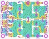
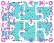
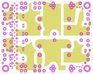
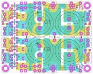
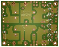
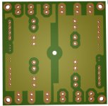
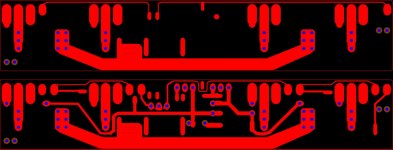
- (AndrewT) added little "island" with two connected pads between pads of diode "snubber" capacitor C5-c12. This way Builder have option:
- (Keantoken) Rearranged rectifier diodes and snubber capacitors, space between back to back TO-220 diodes is 5mm now. I think best option for mounting is using spacer, this way we have mechanical rigidity & good cooling.
- (James) CS1,CS2,C13,C14 now have 6mm allowed width if mounting on top
- (James) All little element pads ("donuts") are enlarged
- (James) Added dedicated discharging resistors RD1&RD2 (resistor&LED not enough for discharging, James?)
to be continued...
- to use snubber caps only (island is disconnected). Pin spacing is 5mm and mounting is possible top&bottom.
- to use additional resistor in series with capacitor: One leg of resistor/capacitor is connected to island and other leg is connected to pads of original snubber capacitor. In this case resistor and capacitor are mounted on the bottom of the board. Pin spacing is about 3.5mm for both resistor&capacitor.
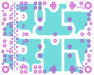
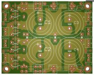
- (Keantoken) Rearranged rectifier diodes and snubber capacitors, space between back to back TO-220 diodes is 5mm now. I think best option for mounting is using spacer, this way we have mechanical rigidity & good cooling.
- (James) CS1,CS2,C13,C14 now have 6mm allowed width if mounting on top
- (James) All little element pads ("donuts") are enlarged
- (James) Added dedicated discharging resistors RD1&RD2 (resistor&LED not enough for discharging, James?)
to be continued...
Attachments
Last edited:
James:
- Resistors in ground tracks. 2 reason against:
- Resistor between rectifiers and first cap.
I'll think about it. I can shrink first cap to 30mm and put pads similar between P1-P4 but shorter. Maybe.
- Resistors in ground tracks. 2 reason against:
- Not enough space.
- Eventual position on board is between Caps, very impractical for changing
- Resistor between rectifiers and first cap.
I'll think about it. I can shrink first cap to 30mm and put pads similar between P1-P4 but shorter. Maybe.
- Resistor between rectifiers and first cap.
I'll think about it. I can shrink first cap to 30mm and put pads similar between P1-P4 but shorter. Maybe.
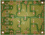
Done with additional rearrangements.
All please check one more time.
Attachments

I think you've got everything covered now -
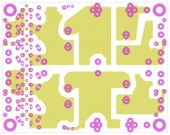
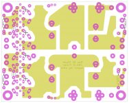
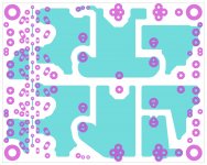
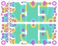
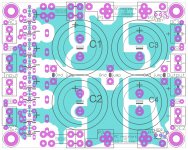
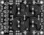
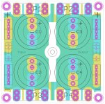
I see the short blue tracks under the caps C5 - 12 for R+C across the diodes? It's getting pretty busy in that area now!
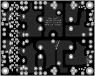
From the writing on the 5th thumbnail, the yellow colour is the bottom layer, yes?
Aah, found the discharge resistors RD1 & RD2, hidden next the output terminals and I see you've moved the leds to the corners - neatly done, that.
I see the short blue tracks under the caps C5 - 12 for R+C across the diodes? It's getting pretty busy in that area now!
From the writing on the 5th thumbnail, the yellow colour is the bottom layer, yes?
Aah, found the discharge resistors RD1 & RD2, hidden next the output terminals and I see you've moved the leds to the corners - neatly done, that.
Could you do one last addition? if looking at the left hand thumbnail, could you add a donut directly below the "P1" terminal just inside the edge of the ground plate of C1, C3 (and a clearance hole on top plate between C2 and C4) and clearance space on the bottom plate - it'll enable a simpler setup to add a series resistor between the gnd terminals of C1 <-> C3 by cutting a groove across that ground plate (for C2 <->C4, it's the opposite with clearance hole on top plate and donut on bottom plate) - probably not often used but if simple to add, would like the possibility - it'll also make better use of that central "Gnd jump' donuts
.... and I've finally run out of things to say!! Thanks for your patience.
.... and I've finally run out of things to say!! Thanks for your patience.
Ordered (this time in black).
I'll wait a little before enable order for others, want to be sure there are no manufacture problem with the board.
Manufacturing done, no problem
") . Shipped.
. Shipped.Ordering enabled.
Dirt Cheap Dirty Boards Order page
10(+-2) Pieces 25$ free shipping, color is your choice
Attachments

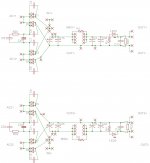
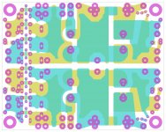
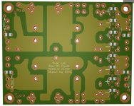
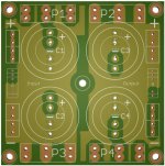
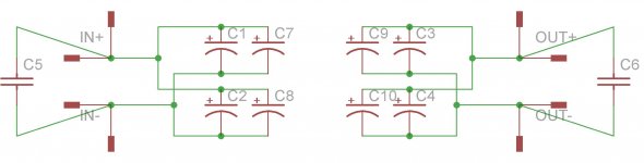
A little teaser for you guys, 10x10 power supply for power amps - one rail - with CR(LC) filter, symmetric resistors on +&- side, without rectifiers, plan is to use high power bridge or special rectifier board.
This is kind of modular, you can use 2 or 3 per rail for real high power filtering & optionally connect R or L between boards (jump filter connections on boards).
Question is how much current is possible through PCB traces (1 oz PCB thickness)?
Attachments
Last edited:
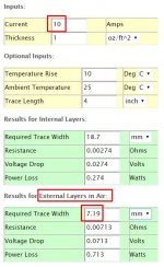
That 7.19mm shared between top and bottom (external) layers of 0.142 wide traces for 10A continuous gives a 10C deltaT and 71.3mV drop along the trace.
You could check this with a DMM while the amp is delivering maximum power.
BTW,
I have laid out a 2pair output stage for a 100W into 8ohms amplifier using a 160thou trace top & bottom and it too is just under 4" long.The PCB is ~149.7mm long
You could check this with a DMM while the amp is delivering maximum power.
BTW,
I have laid out a 2pair output stage for a 100W into 8ohms amplifier using a 160thou trace top & bottom and it too is just under 4" long.The PCB is ~149.7mm long
Attachments
Last edited:
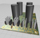
Some time ago, there was a small neat little board with 4 off TO-220 diodes that mounted to a flat sided heatsink that could be clamped down with those transistor clamp bars - 1 screw per 2 diodes @ 28mm spacing I think, from memory - 2 diodes each side - I think it's a Peter Daniels design, very neat, like all his gear - it came with a power supply board similar to this one you're now doing
I generally use a 'building block' (module) of the 4 diodes on a common heatsink, that includes the C+R//C snubber and series 3W SMD resistors either on the input to the diodes (secondary winding damping) or before the first cap (larger conduction angle/reduced pulse amplitude) - some people seem to find the C+R across the diodes useful too, like in your present boards at DirtyPCBs
Another 'building block module' I use is a basic C-Multiplier in place of the 'R' in a C-R-C filter in power amps (=> C-CMx-C) - not sure if this is of much interest but of great value instead of chokes ....
I must ask (Prof) Ed Cherry about this zigzagging tracks on pcbs - I don't recollect any details about it that Andrew indicated but he's addressing the AES meeting next month about amplifier design, so I'll ask, unless you have access to the paper in question?
- Status
- This old topic is closed. If you want to reopen this topic, contact a moderator using the "Report Post" button.
- Home
- Amplifiers
- Power Supplies
- 10x8 Raw DC board with CR(L)C filter