With 10k series resistance we usually start to see stability problem (and needs compensation caps here and there..). I think it's okay with 36x or 40x as shown below:
20k/680=29x
20k/620=32x (original gain value)
20k/560=36x
20k/500=40x
20k/470=43x
Going to try 20k and 550R (220R+330R)
I am building second board and dont have 12v Zeners but have 14V - is it going to work with 14v's?
Going to try 20k and 550R (220R+330R)
I am building second board and dont have 12v Zeners but have 14V - is it going to work with 14v's?
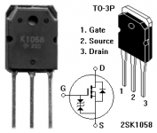
You don't need the zeners or the diodes on the outputs. Those are built into the lateral MOSFETs. Those are only needed for vertical MOSFETs. You can just leave those out.
Attachments
Last edited:
I am building second board and dont have 12v Zeners but have 14V - is it going to work with 14v's?
I don't use protection diode for LATFET amps. But I'm not 100% sure either if the internal diodes will function as promised...
The maximum voltage allowable between Gate and Source is (+/-) 15 Volts, so 14 Volt zener will protect Vgs from reaching above 14 Volt.
The integrated Zener+Diode will have a current limit.You don't need the zeners or the diodes on the outputs. Those are built into the lateral MOSFETs. Those are only needed for vertical MOSFETs. You can just leave those out.
If used with a low value gate stopper you could damage the Zener+Diode, when there is an incident.
I advise using a higher value gate stopper and/or using an external Zener+Diode protection.
The Zener+Diode must be <15V. It's specified as absolute maximum for the lateral mosFETs.I don't use protection diode for LATFET amps. But I'm not 100% sure either if the internal diodes will function as promised...
The maximum voltage allowable between Gate and Source is (+/-) 15 Volts, so 14 Volt zener will protect Vgs from reaching above 14 Volt.
Most use a 12V Zener + 0.7V Diode giving 12.7V at moderate bypass current.
Check the mosFET datasheet to see what current can pass through the Drain when Vgs = 12.7Vgs.
Id is off the top of the graphs.
Last edited:
You don't need the zeners or the diodes on the outputs. Those are built into the lateral MOSFETs. Those are only needed for vertical MOSFETs. You can just leave those out.
That's not entirely true. Current Semelab lateral MOSFET devices don't have internal protection diodes. Exicon double die lateral MOSFETS also don't have internal protection diodes.
FX8 in Stereo
Thanks for clearing up that whole Zener diode thing. I guess I found out that it works fine with it and affords extra external protection for these pricey lateral FETs.
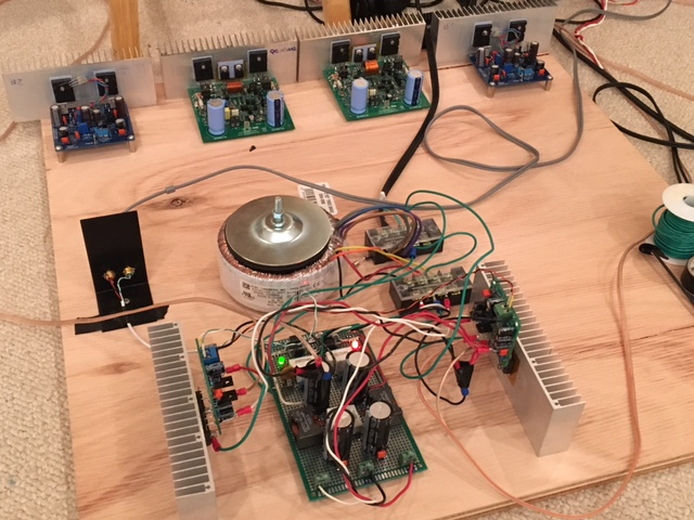
I built up the second unit and adjusted gain to be 36x (20k/550R) and this gain is perfect - great dynamics and no audible distortion. I was missing a 1k pot so used a 5k pot and found that you really have to twist on the screw to get the right bias. When I first turned it on I had 25v across the 10ohm external safety resistor and it took a lot of turning to get it to 1v for 100mA bias.
Listening to it now, maybe on 5 tracks total, so far, very very good amp - actually, excellent amp. Very happy with it. Stereo sounds great.
You can see this is the test bed with a Dx and inverted JFET Circlophone in background.
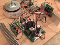
Closeup of FX8:

Thanks for clearing up that whole Zener diode thing. I guess I found out that it works fine with it and affords extra external protection for these pricey lateral FETs.
I built up the second unit and adjusted gain to be 36x (20k/550R) and this gain is perfect - great dynamics and no audible distortion. I was missing a 1k pot so used a 5k pot and found that you really have to twist on the screw to get the right bias. When I first turned it on I had 25v across the 10ohm external safety resistor and it took a lot of turning to get it to 1v for 100mA bias.
Listening to it now, maybe on 5 tracks total, so far, very very good amp - actually, excellent amp. Very happy with it. Stereo sounds great.
You can see this is the test bed with a Dx and inverted JFET Circlophone in background.
Closeup of FX8:
Attachments

Last edited:
I advise using a higher value gate stopper and/or using an external Zener+Diode protection.
Yes, I like the idea of using external diode protection. But I prefer a compact PCB/layout so I have to leave the protection out (my PCB is smaller than X's PCB)...
What value do you suggest for gate stopper? I honestly prefer as small as possible tho...
Yes, I like the idea of using external diode protection. But I prefer a compact PCB/layout so I have to leave the protection out (my PCB is smaller than X's PCB)...
What value do you suggest for gate stopper? I honestly prefer as small as possible tho...
Please show us a photo if your amp is indeed smaller than 50mm square. Did you go to SMT parts or just turn on resistors and diodes on end with a long leg from the top? I don't see how you can squeeze this much smaller (leaving off 4 diodes doesn't make it that much smaller).
With +/-42vdc you can't use BD139 and BD140 devices in VAS.
You can expect about 80W.
ok thanks.. i will use then MJE340/350 as like FX9. anything else?
Attachments
ok thanks.. i will use then MJE340/350 as like FX9. anything else?
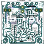
That's a nice layout - sans zeners. Are the extra holes under the pot for different types of pot pinouts?
Can you share the Sprint file?
Thanks.
That's a nice layout - sans zeners. Are the extra holes under the pot for different types of pot pinouts?
Can you share the Sprint file?
Thanks.
that extra holes are for fixed bias resistor after adjustment thru trimpot.
Attachments
Please show us a photo if your amp is indeed smaller than 50mm square.
Unfortunately I don't have the required software to connect my Samsung to computer, so no pictures for now...
Did you go to SMT parts or just turn on resistors and diodes on end with a long leg from the top? I don't see how you can squeeze this much smaller (leaving off 4 diodes doesn't make it that much smaller).
If I can get 1/8W resistors then that is my preferred size. But no SMD here... For series FB resistor I intentionally use 1W... Compensation caps (Miller's) are always direct on TR pins below PCB... This time zobel is below PCB to avoid trace inductance...
I consider the estate around the driver and mosfet very important, so no protection diodes there...
I am not an amplifier Designer, but I read extensively.
Other prominent Designers suggest that
Vertical mosFETs need gate stoppers roughly 22r to 150r
Lateral mosFETS need gate stoppers roughly 47r to 470r.
Latfet amps IMO tend to have insufficient "drive". This is what makes it's design hard... Even tho not critically, gate stopper (and especially source resistors) will only worsen this. As long as oscillation is taken care of by providing less loop area around gate and source (less parasitic inductance/capacitance), the gate stopper can be made smaller...
Can you give guidance on the layout of the three wires/traces to feed the output mosFET?................ As long as oscillation is taken care of by providing less loop area around gate and source (less parasitic inductance/capacitance), the gate stopper can be made smaller...
Can you give guidance on the layout of the three wires/traces to feed the output mosFET?
Nothing special, only shortest trace possible. Easier when the latfet is arranged in "90 degree" ala First-One or PeeCeeBee V2. Sometimes I used 1/8W resistor directly on the gate pin hanging above PCB (P2P).
I too attach the base/gate stopper directly to the base/gate pin and close to where the lead out exits the package.
But you said
But you said
and now just keep them short !less loop area around gate and source
Jay,
It's really not that hard to get an image from your camera or phone onto your computer for sharing your diy world. I have heard that lack of software between your Samsung and your PC numerous times and just seems odd that someone as skilled and resourceful as you would let something like that stop you. It's a USB cable or whatever and drag and drop a jpg file to a folder. Then upload to diyAudio as attachment. Not that hard. So a description of your methods to get the PCB smaller are somewhat achievable in words - as they say though, a picture is worth a thousand words. Many people would benefit from seeing how you actually achieve this. Case in point, me, and AndrewT with this recent discussion of wiring traces and gate stoppers around outputs.
I really hope you put some effort to getting photos added to your posts. It would help a lot. But if you just don't want to share images - that's your prerogative but let's not blame Samsung.
But you said <snip> and now just keep them short !
Sorry, I think I've probably used the wrong words when I said "loop area"...around Vgs... Compact layout should minimize this area.
- Home
- Amplifiers
- Solid State
- 100W Ultimate Fidelity Amplifier