Hi Mile,
The A IRFP is singing. However it need a little help. See attached scope shots. Looks like it needs compensation changes.
Blessings, Terry
Is it connected to load that has capacitive component? I had seen such overshoot in one of the amps (PEECEEBEE tests by Thimios- http://www.diyaudio.com/forums/solid-state/231662-peeceebee-175.html#post4209696) that had capacitive +resistive load.
reg
prasi
Hi Mile,
The A IRFP is singing. However it need a little help. See attached scope shots. Looks like it needs compensation changes.
Blessings, Terry
Nice work, you can change compensation C10 220pF to 470pF, C11 22pF to 100pF and C12 15pF to 22pF...
Regards
Still4,
could you add one capacitor change at a time and post your heavily damped overshoot results for each single change?
And then all three added together?
This type of overshoot is very typical of the last few amps I have built and although I can reduce them slightly, I seem to be unable to remove completely. I seem to be adding the comp adjustment in the wrong place.
Then when I add a tiny bit of load capacitance the not properly compensated amp rings badly.
Seeing the results of three different comps may help me understand what's happening in my amps. 4 in a row had similar bad behaviour. The most recent NX is the first in over a year to not show this.
Still4,
Yes, go-step-by step with compensation mentioned by AndrewT,
we must firstly compensate the over-shoot a little bit,
then eliminate one half-period of settling time, but not decreasing SR so much in same time
sistem is now PI(D), with integrator @cca 5,8-6usec (cca 170KHz)
micro-diferenciator is our roll-off BW
The amp is fast (look the settling time), and this is OK!
1. C12
-if you can, put C12 to the other side of the R15 (not to out of OP-AMP, but involving the 47R in the local compensation), !then look at scope!
-then increase C12 by 4p7F then by 10pF... !every change made - look at scope!
2. C11 is our roll-off but also is involved in "I" constant,
-put in series with C11 10K, !look at scope!")
-increase C11 by 22pF then another 47pF and so one... !look ...!
3.At last you must change C10 and/or R21, this is the dumping comp for "I" freq, put 470pF, then try with 1nF leaving R21 unchanged.
With best result then we must trimming R21 to ideal scope response
Edit:
This is a prototipe directly from simulation we played with Mile (Apex), and it`s promising...
for one mosfet pair the PSU is cca +/-(40)42-45VDC
The OP-AMP use floating supply referencing to the amp output
and is also boot-strapped so we can drive (with one IC cca 35mAp-p) directly the output stage to klipping (PSU - 2VDC)
Regards, Dragan
Yes, go-step-by step with compensation mentioned by AndrewT,
we must firstly compensate the over-shoot a little bit,
then eliminate one half-period of settling time, but not decreasing SR so much in same time
sistem is now PI(D), with integrator @cca 5,8-6usec (cca 170KHz)
micro-diferenciator is our roll-off BW
The amp is fast (look the settling time), and this is OK!
1. C12
-if you can, put C12 to the other side of the R15 (not to out of OP-AMP, but involving the 47R in the local compensation), !then look at scope!
-then increase C12 by 4p7F then by 10pF... !every change made - look at scope!
2. C11 is our roll-off but also is involved in "I" constant,
-put in series with C11 10K, !look at scope!
-increase C11 by 22pF then another 47pF and so one... !look ...!
3.At last you must change C10 and/or R21, this is the dumping comp for "I" freq, put 470pF, then try with 1nF leaving R21 unchanged.
With best result then we must trimming R21 to ideal scope response
Edit:
This is a prototipe directly from simulation we played with Mile (Apex), and it`s promising...
for one mosfet pair the PSU is cca +/-(40)42-45VDC
The OP-AMP use floating supply referencing to the amp output
and is also boot-strapped so we can drive (with one IC cca 35mAp-p) directly the output stage to klipping (PSU - 2VDC)
Regards, Dragan
Last edited:
I forgot,
C13 is now 2,2uF, and is too small for maintaining IC bootstrap near max power or klipping point
use 100 - 220uF/40V
C5, C4 are there for stability of proper biasing (CVS) use 22uF/35V instead of 2,2uF
R13, R14 must be 2W resistors
D3,D4 must be in contact with heatsink or mount them on the face on output devices,
here you can use some TO 220 or SOT 32 (TO 126) BJTs in diode arrangement
Dragon,I forgot,
C13 is now 2,2uF, and is too small for maintaining IC bootstrap near max power or klipping point
use 100 - 220uF/40V
C5, C4 are there for stability of proper biasing (CVS) use 22uF/35V instead of 2,2uF
R13, R14 must be 2W resistors
D3,D4 must be in contact with heatsink or mount them on the face on output devices,
here you can use some TO 220 or SOT 32 (TO 126) BJTs in diode arrangement
Typing is waaaaaaay easier than soldering. So is sim work. This is what I did so far. I didn't move C12 BTW.
Attachments
-
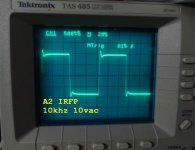 A2 IRFP 10KHZ.jpg44.1 KB · Views: 992
 -
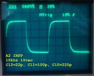 A2 IRFP 10KHZ C10=470, C11=100, C12=22.jpg97 KB · Views: 142
 -
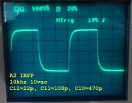 A2 IRFP 10KHZ C10=220, C11=100, C12=22.jpg101.5 KB · Views: 123
 -
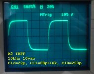 A2 IRFP 10KHZ C10=220, C11=68+10K, C12=22.jpg95.7 KB · Views: 912
 -
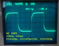 A2 IRFP 10KHZ C10=220, C11=47+10K, C12=22.jpg97.6 KB · Views: 924
 -
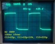 A2 IRFP 10KHZ C10=220, C11=22+10K, C12=22.jpg100.6 KB · Views: 956
 -
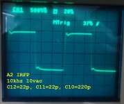 A2 IRFP 10KHZ C10=220, C11=22, C12=22.jpg98.1 KB · Views: 984
This is a prototipe directly from simulation we played with Mile (Apex), and it`s promising...
I'm played too with it, in the simulator. Very simple driver stage even for high power application. MC2 audio use it.
Sajti
Dragon,
Typing is waaaaaaay easier than soldering. So is sim work. This is what I did so far. I didn't move C12 BTW.
..at 10khz, is the treble cut a bit larger? Is there a way to know the frequency range..

Terry did you test the sound before/after modding the compensation?
Maybe its not correlating with a nice scope result...
(Exception: when the amplifier is not stable of course...)
I have not but I can easily do that because I have only changed one channel. I can hook it up to my system and A/B one side against the other.I'll try to do that in the morning.
..at 10khz, is the treble cut a bit larger? Is there a way to know the frequency range..
Square way is for SR and stability test, with sinus way or audio signal BW is from 5Hz up to 50kHz.
Dragon,
Typing is waaaaaaay easier than soldering. So is sim work. This is what I did so far. I didn't move C12 BTW.
Yppp, i agree with you Still4, playing with sim and/or typing is way easier than soldering.
But soldering in the other way is all one can do if there is no background what to sim or type.
BTW, I`m more active here, look my ClassA with IC`s with auto adaptiv bias or some ather fully documented projects.
And trust me, for me is muuuuch mooore complicated to answer/typing to you in english then do some new projects or bether,
... do whole ideas, sim-ing...!
BTW, Apex invited me to helps you for fine trimming comp in this A2 project, he has no time at the moment!
With fast amps is much harder to do some good/proper comp, with slow one there is no such thing to do,
is just compensated and thats all!
And then redo comp with some reactive load!!!
------------------------------------
Scope graf with C12=22pF, C11=47pF+10K, C10=220pF looks good, but sligthly to mach comp.
Try to use C11=33pF(27pF)+10K, then playing with that R +/- (use a trimmpot 100K)
a little bit to achive only an small overshoot (read the trimmpot value - take nearest stnd R)
At last you must play with C10+R21, for R21 use the same trimmpot 100K, with C10: 220pF - 470pF - 1nF
The goal is achive square with fast SR, no or just little overshoot, no settling osc period/half period and no osc with 8R0//220nF reactive load.
Regards Still4, keep doing nice works
Dragan
EDIT: try move that C12
Last edited:
With fast amps is much harder to do some good/proper comp, with slow one there is no such thing to do,
is just compensated and thats all!
Which opamp do You recommend?
Sajti
The goal is achive square with fast SR, no or just little overshoot, no settling osc period/half period and no osc with 8R0//220nF reactive load.
With this A2 we are limited/narrow in BW, so don`t expect "perfect" square wave response @10KHz ( or even @ highest freq ),
for that we need plenty of high harmonics, at lest 7-9,
and this for 10Khz square response means at least 100KHz BW or even more.
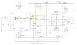
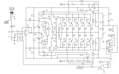
Look at this variation of A2,
uses double OPA2134 for cca +/-70mAp-p drive for output stage (more mosfet pairs, "taught gate charge" ,highest dI/dt drive, ...etc!)
and the gabarits/dimensions and price are same, but now we can lower the gain of "VAS" stage, with acquisition in wider BW.
In front there is LME49710 with stnd +/-15-18VDC supply respect to GND, with tree functions, input buffer with gain,
control local NFB, and most important global NFB-PID supervisor with excellent performans.
Now we got almost 370KHz BW @(-3dB) roll off, plenty for needed high harmonics and good BW for much better square wave response.
Phase in audio section is flat 0° +/- 2-3°
THD is about 0,001% @1Waverage (we call this RMS
) with 8R0 non-reactive load.Input voltage noise is under 10nV/sqrt(Hz) like preap
SNR 106dB@1KHz
PSSR more than (-)105dB on both pos and neg rails 100Hz ripple
Klipping almost at supply rails.
Attachments
I'm played too with it, in the simulator. Very simple driver stage even for high power application. MC2 audio use it.
Sajti
-is there floating-bootstraped opamp driver supply respect to output
-please, share schematics detail of MC2 (no need for entire circuit sch)
Regards
Dragan
Yppp, i agree with you Still4, playing with sim and/or typing is way easier than soldering.
But soldering in the other way is all one can do if there is no background what to sim or type.
BTW, I`m more active here, look my ClassA with IC`s with auto adaptiv bias or some ather fully documented projects.
And trust me, for me is muuuuch mooore complicated to answer/typing to you in english then do some new projects or bether,
... do whole ideas, sim-ing...!
BTW, Apex invited me to helps you for fine trimming comp in this A2 project, he has no time at the moment!
With fast amps is much harder to do some good/proper comp, with slow one there is no such thing to do,
is just compensated and thats all!
And then redo comp with some reactive load!!!
------------------------------------
Scope graf with C12=22pF, C11=47pF+10K, C10=220pF looks good, but sligthly to mach comp.
Try to use C11=33pF(27pF)+10K, then playing with that R +/- (use a trimmpot 100K)
a little bit to achive only an small overshoot (read the trimmpot value - take nearest stnd R)
At last you must play with C10+R21, for R21 use the same trimmpot 100K, with C10: 220pF - 470pF - 1nF
The goal is achive square with fast SR, no or just little overshoot, no settling osc period/half period and no osc with 8R0//220nF reactive load.
Regards Still4, keep doing nice works
Dragan
EDIT: try move that C12
What is the reason for the added 10k resistor?
-is there floating-bootstraped opamp driver supply respect to output
-please, share schematics detail of MC2 (no need for entire circuit sch)
Regards
Dragan
I will play some more, but with BJT output, which looks better to me
MC2 E15/25 output stage schematic attached. This is absolutely the same concept in case of the driver stage.
Sajti
Attachments
- Home
- Amplifiers
- Solid State
- 100W Ultimate Fidelity Amplifier