Here, I plan to get more negative feedback like JLE but don't have time yet
Attachments
Last edited:
Back in 2020 I was looking at using the tpa3255 in my 3 way mfb design but shelved it at the time because I couldn't get the heat-sinking done right. Was using tpa3116 based amps before and wrongly assumed this bigger brother would accept the same cooling solution 👎 below the 3116 design with one 3116 doing mid and highs and one in pbtl doing bass:
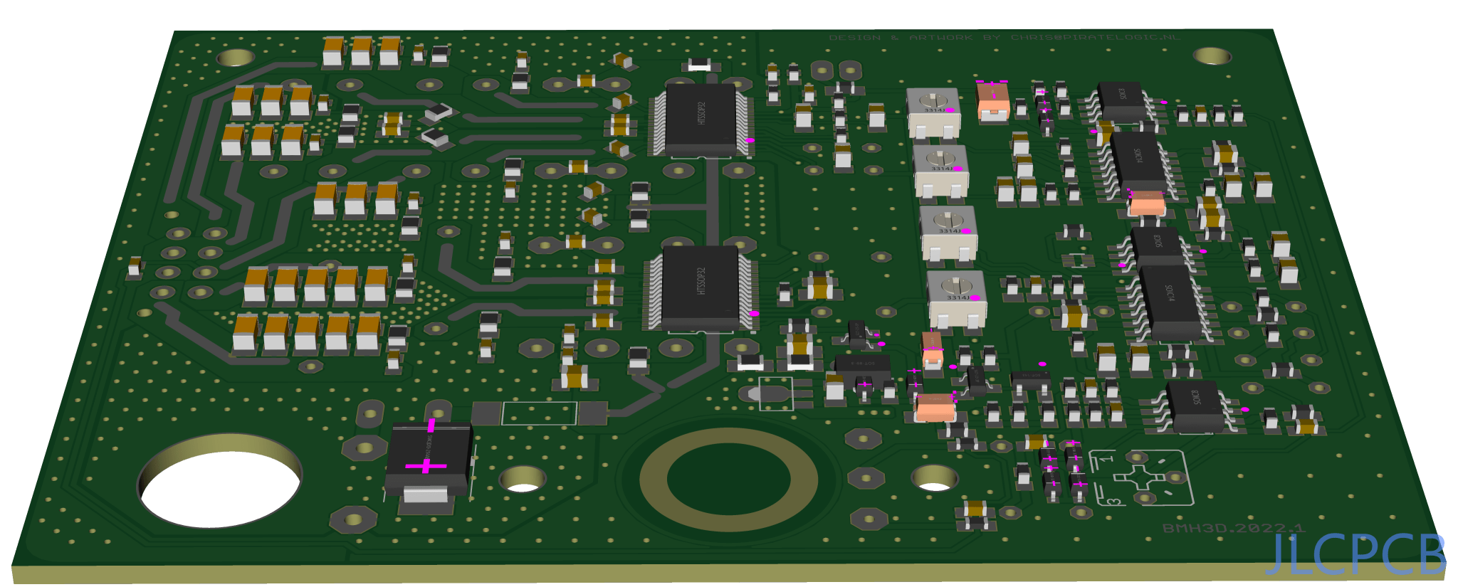
My 2020 version with TPA3255 in 2:1 mode, BTL bass single ended mid and high.
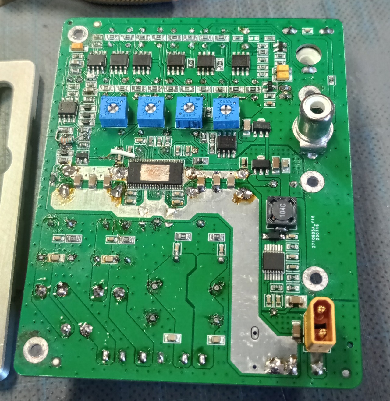
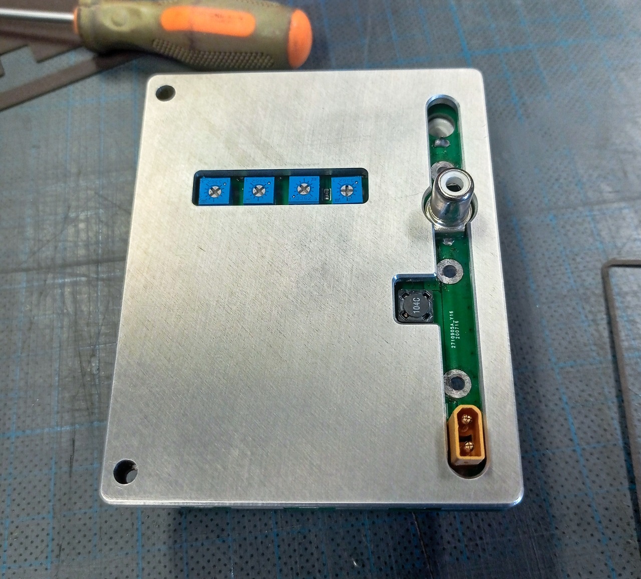
A few weeks ago I visited a fellow builder who helped me addressing the cooling problem with his CnC and a piece of 6mm aluminum, top side:
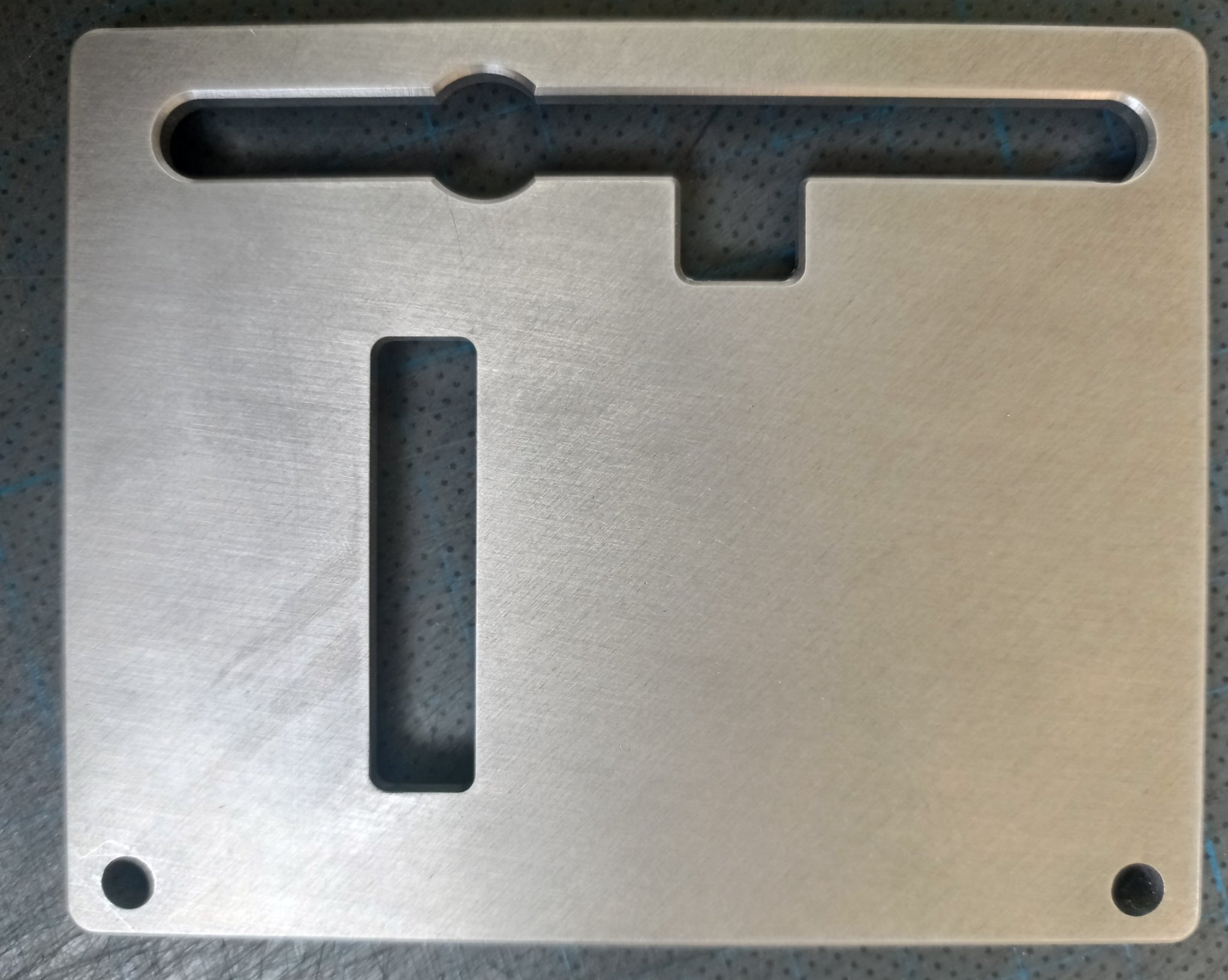
And the bottom side with a small stud to connect to the tpa3255 exposed die:
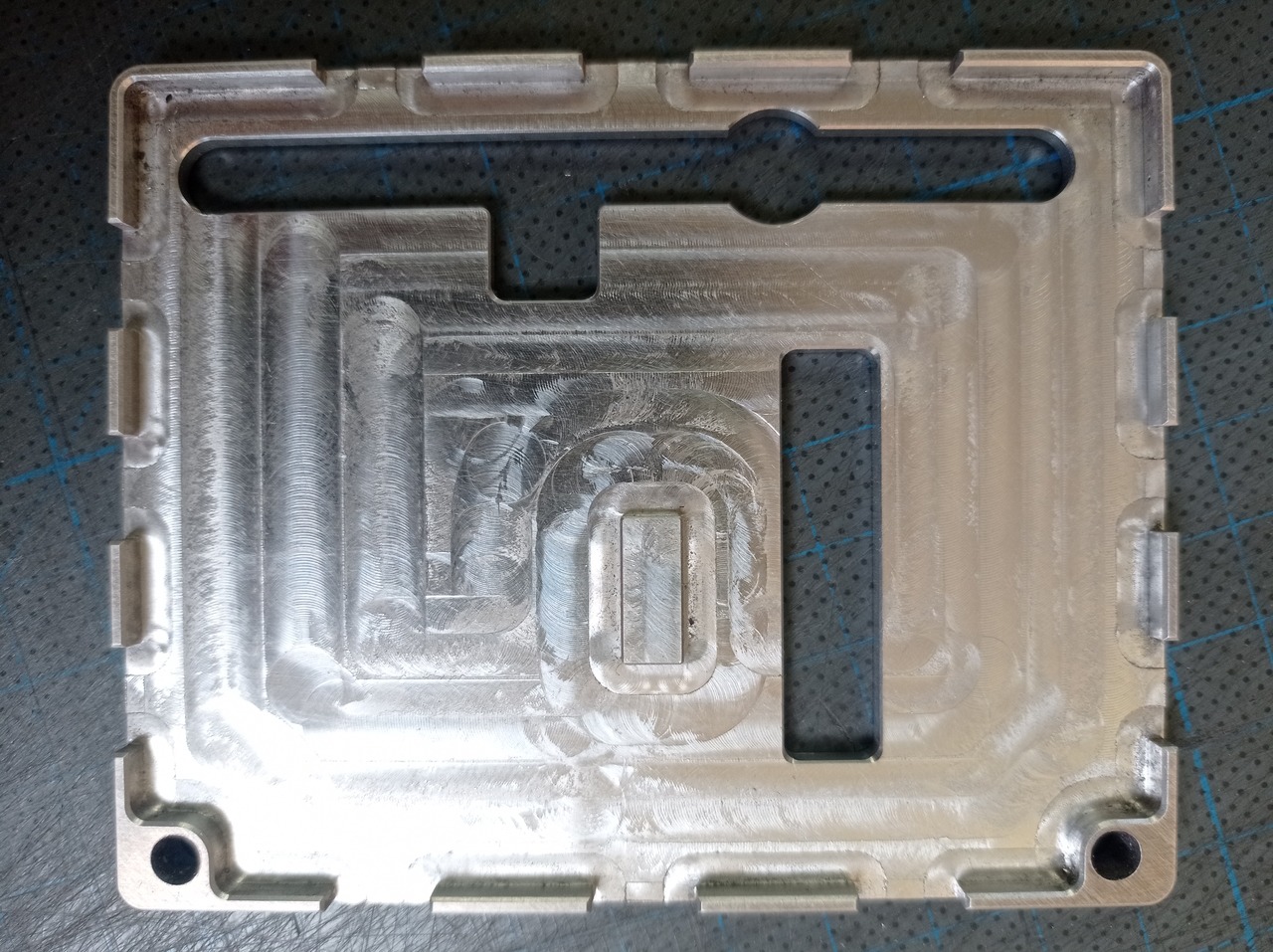
Tight fit for a prototype, I just love CnC.
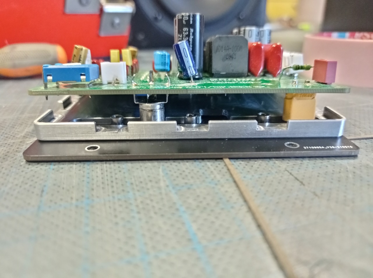
The alu cooler gets sandwiched between the pcb and frontplate with a little thermal grease on top of the tpa
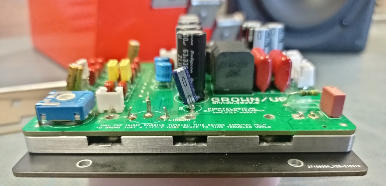
The slots are for aiding natural convection and are placed both top and bottom as well on the sides
topside
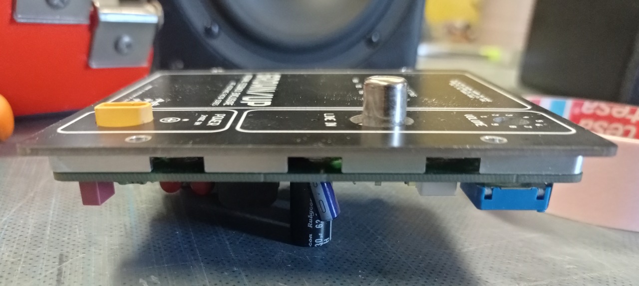
Did some tests yesterday - sorry neighbors - and was able to keep the heat sink below 50C with Vdd 51V and a 8 ohm woofer, still a little too hot to my taste but the good thing is that it didn't go into thermal protect anymore. Still considering putting a rectangular 50x50x15mm heatsink on top of the cooler to extend the life of the 105C electrolytics. Ignore the 24V 4A psu text, am still working on the silkscreen design 😎
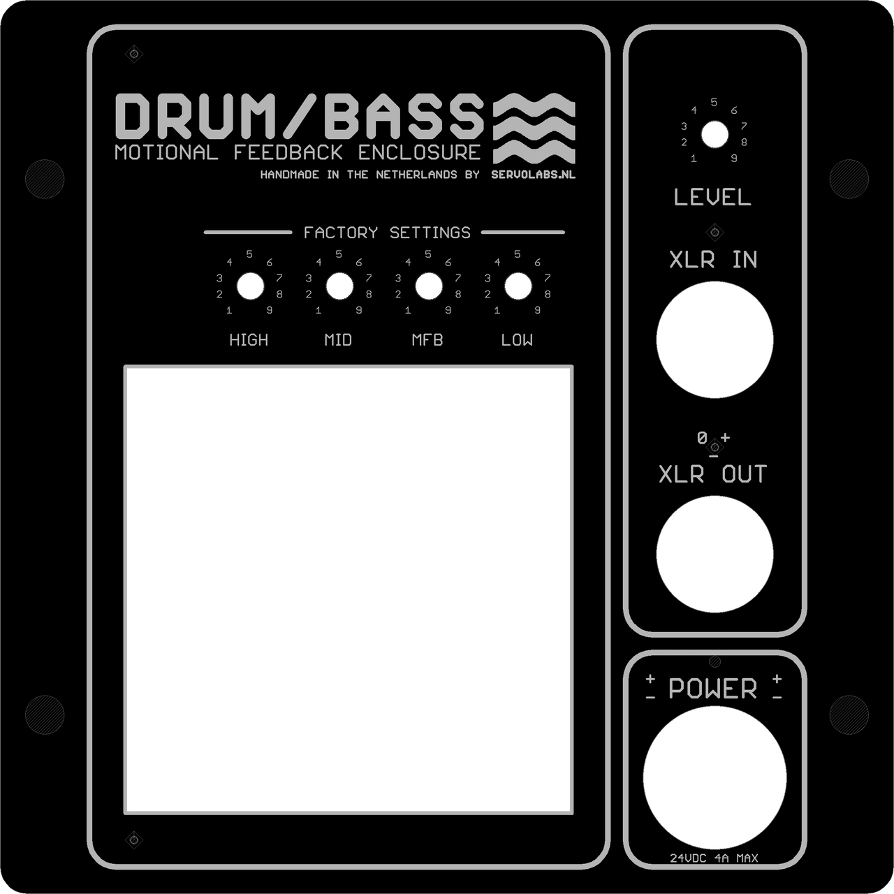
A last word to the webdev, been some time since I posted here and am thrilled by your new editor ! specially the image handling is great !!
WELL DONE 👍👍👍
My 2020 version with TPA3255 in 2:1 mode, BTL bass single ended mid and high.
A few weeks ago I visited a fellow builder who helped me addressing the cooling problem with his CnC and a piece of 6mm aluminum, top side:
And the bottom side with a small stud to connect to the tpa3255 exposed die:
Tight fit for a prototype, I just love CnC.
The alu cooler gets sandwiched between the pcb and frontplate with a little thermal grease on top of the tpa
The slots are for aiding natural convection and are placed both top and bottom as well on the sides
topside
Did some tests yesterday - sorry neighbors - and was able to keep the heat sink below 50C with Vdd 51V and a 8 ohm woofer, still a little too hot to my taste but the good thing is that it didn't go into thermal protect anymore. Still considering putting a rectangular 50x50x15mm heatsink on top of the cooler to extend the life of the 105C electrolytics. Ignore the 24V 4A psu text, am still working on the silkscreen design 😎
A last word to the webdev, been some time since I posted here and am thrilled by your new editor ! specially the image handling is great !!
WELL DONE 👍👍👍
Last edited:
Hello all. I got this 6 channel tpa3255 amp from. Aliexpress to use in an active 3 way stereo setup.I am using a biamp nexia as a crossover.
Problem is I am getting a strange sound through all the speakers. It's not hum, pink or white noise but a kind of digital background noise.
Sound does not change with volume, does not change if I disconnect signal or turn off the crossover.
It does go away if I unplug all of the inputs though.
Problem is I am getting a strange sound through all the speakers. It's not hum, pink or white noise but a kind of digital background noise.
Sound does not change with volume, does not change if I disconnect signal or turn off the crossover.
It does go away if I unplug all of the inputs though.
Attachments
^^ I don't have answer for you but I was thinking of purchasing this 6 channel for an active amplifer setup also. Please report back if you found and/or fix the problem. Maybe check solder joints to and from inputs. Maybe they just need to be cleaned up. I don't know
I will definetly do that. Seems to be an issue with the input. It has a very small single plug for all six inputs. 8 pins total, six for inputs and to ground pins.
Wondering if it can be an issue that all three tpa3255 chips are all sharing the same ground at the input stage ?
Wondering if it can be an issue that all three tpa3255 chips are all sharing the same ground at the input stage ?
I purchased a few tpa3251 aliexpress boards and they seem to idle around 2W @32V, which is way outside the specified 0.5W.I have the 3251 from 3e but haven't measured it. The 2.5W mentioned in the datasheet is idle loss for the chip itself and there is a note mentioning that output inductors can increase that. There also is another dc-dc converter that's always on on-board for the 12v supply and input buffers, and the buffers probably have some power consumption as well.
And then, based on how quiet your pre-amp/dac is the amp is probably never idle so the reset switch plus lower voltage power supply or even a relay driven by your pre-amp/dac would help a lot.
Not good for battery operation!
Did anyone else measure their 3255? I am a bit suspicious that the chip on my board is not a 3251 but in fact the more power hungry model...
Before uttering wrong conclusions you better study the data sheet.I purchased a few tpa3251 aliexpress boards and they seem to idle around 2W @32V, which is way outside the specified 0.5W.
Not good for battery operation!
Did anyone else measure their 3255? I am a bit suspicious that the chip on my board is not a 3251 but in fact the more power hungry model...
It is ~2W including the step down regulator that I believe powers the op-amps, and indeed there seems to be a hot spot around there when viewed on a thermal camera.Did you measure just the tpa3251 or the tpa3251 plus the 12 volt regulator and the opamps, the 3.3 volt regulator, leds etc. 2 watts idle is not a lot for a 100-600 watt amplifier.
The data sheet actualy says 1W idle in stereo, the 0.5W figure was for 4 channel mode. So... maybe that step down regulator wastes 1W somehow. Makes sense but I think it could be improved a lot with better components.
I will definetly do that. Seems to be an issue with the input. It has a very small single plug for all six inputs. 8 pins total, six for inputs and to ground pins.
Wondering if it can be an issue that all three tpa3255 chips are all sharing the same ground at the input stage ?
Is there a computer nearby or is a computer supplying the audio? It sounds like demodulated RF to me and computers are often rather noisy in that regard.
The RF emissions would be picked up by the input cable and brought into the board where input stage non-linearities convert it into audible (audio band) sounds.
Almost Fixed it. I just lift up the power supply and it almost completely stopped.
It was sitting on top of the biamp nexia and must have been creating some kind of ground loop.
With a 12v power supply the same noise exists but its very quiet. As soon as I plug in a 36v power supply it gets louder than the 12v.
It was sitting on top of the biamp nexia and must have been creating some kind of ground loop.
With a 12v power supply the same noise exists but its very quiet. As soon as I plug in a 36v power supply it gets louder than the 12v.
Last edited:
Hello. I received this payment and I have a lot of questions.https://www.aliexpress.com/item/100...yQpguf662PdigT4LKPbEUsjlvh7GRcdgwaXedruFREeTY
Interesting, new product, good base for modification (can use bigger, good quality inductors, bigger size capacitors, etc.)
1. I don't understand why they installed two capacitors connected in series to the pvdd? Why turn on in series and not in parallel, and is it correct to use capacitors at a voltage of 25v? 2. How do they get a 12v voltage on the board if a power transistor is installed instead of a 12v regulator? 3. What kind of switch do they propose to use? (Third photo)
Attachments
Last edited:
@RuslanK35
Just a request from me.
Could you please post high resolution pictures of the top and bottom of your bare circuit board? Thanks in advance.
This is a stupid savings measure. Two 25v capacitors in series give 50v withstand voltage, but the capacitance is halved (4700->2350uF). This doubles the internal resistance of the capacitors. So totally cheap. But you can cut through part of the traces and rewire the capacitor legs on the underside.
They probably built their own switching regulator circuit for cost reasons.
Personally I would remove the 12v supply completely and use a good clean external 12v source eg Meanwell 12v and the SMPS filter from the forum.
Any kind of on/off switch will work.
Thank you for helping me. You asked for a photo of the "bare circuit board". Do you need a photo of the board with soldered elements to see where the tracks go? Or do you just need a high-resolution photo of the board with the elements installed on it? If necessary, I can remove all large elements from the board so that it would be fashionable to see the path of the board tracks.@Roland968
@Roland968 You also wrote that I can change part of the scheme. when you have the necessary photos, could you guide me on the right path to finalize this board?
@RuslanK35
If possible, please take photos with as few elements as possible so that I can see the conductor tracks.
I should then be able to see which traces you need to change.
If possible, please take photos with as few elements as possible so that I can see the conductor tracks.
I should then be able to see which traces you need to change.
Yes, thanks, but you would also need to remove the two large capacitors between the coils and take a picture of the circuit board underneath. These capacitors are presumably also connected in series.It ok?
What is the voltage of these capacitors?
- Home
- Amplifiers
- Class D
- TPA3255 - all about DIY, Discussion, Design etc


