In the last schematic you posted, where G2 is marked at the junction of R4 and C2 is the correct location for audio ground.
D1, D2 and R4 are there to provide a little isolation between audio ground and the power supply ground. R4 would minimize the possibility of ground loops through your interconnects. D1 and D2 are to ensure the ground ring on the RCA connector can't have much more than .6V present for safety.
Thanks for Confirming. I guess the point of my first post was to ask the question if the V2.4 schematic is actually showing the incorrect location for G2.
Which it appears that it is. Can we please ask a forum admin to revise the V2.4 schematic to V2.5 with this change as its very misleading when you are trying to track down a problem
Please add some more details.
Are you saying that where G2 is marked on the original schematic is the signal (Audio) ground?
Because if you are it can't be. Just look at the traces on the PCB, Signal (Audio) ground is located between the junction of R4 and C2. Not on the other side of R4
I don't see the "G2" marking on the PCB, so there is no difference of G2 between the PCB and the schematic.
I guess the question is more what you mean by G2, "audio GND", or "signal GND". In my view, GND is GND is GND (or G1 = G2).
The audio input does not terminate directly into GND to avoid a ground loop formed by the two stereo inputs (as explained by jwilhelm before).
two grounds, the safety ground from the 3 prong IEC inlet connects straight to the nearest metalwork preferably at the IEC mounting screw...this ground has nothing to do with the rest of the circuit grounding as this is meant to protect the operator from shock hazards...
now the psu grounds must connect to the chassis at a point where signal is lowest, and that is at the input...
now the psu grounds must connect to the chassis at a point where signal is lowest, and that is at the input...
Everyone agrees that there is a ground for the input (say audio ground) and a ground for the remaining circuit (say power supply ground). These are seperated by R4 (4.7R resistor) for reasons stated before.
This is clearly indicated on the schematic and I have hand drawn it, a few post back.
The schematic however needs updating for the following reasons.
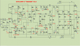
1. On the left hand side of the schematic the "power supply" ground is labelled G2 and on the right hand side it's labelled G1. No matter how you justify this, it is wrong and misleading. Show me another schematic that labels the same point with two different names.
2. The schematic does not show the optional configuration(s).
3. On the DIYAUDIO store site there are two different schematics, which can lead to confusion for new builders.
Changing the post to a more serious subject, so we don't get bogged down with semantics.
I have noticed that some of the builders (not all) are experiencing oscillation at the input stage. One builder, a few posts back, had to remove the capacitor across the zener diode to stabilise the circuit and Stuart has a small oscillation at start up, on one channel, which eventually dissappears.
Has anyone investigated this or tried to modify the cct?
As an example I have had a look at the PCB and in my opinion the "audio" ground track is too long. Note I'm not saying that this is the cause of oscillation.
I know that no two builds are the same and that there are many variables however I'm open to your ideas and suggestions, especially from people that have built this amp. Tony etc?
Regards
Harry
This is clearly indicated on the schematic and I have hand drawn it, a few post back.
The schematic however needs updating for the following reasons.
1. On the left hand side of the schematic the "power supply" ground is labelled G2 and on the right hand side it's labelled G1. No matter how you justify this, it is wrong and misleading. Show me another schematic that labels the same point with two different names.
2. The schematic does not show the optional configuration(s).
3. On the DIYAUDIO store site there are two different schematics, which can lead to confusion for new builders.
Changing the post to a more serious subject, so we don't get bogged down with semantics.
I have noticed that some of the builders (not all) are experiencing oscillation at the input stage. One builder, a few posts back, had to remove the capacitor across the zener diode to stabilise the circuit and Stuart has a small oscillation at start up, on one channel, which eventually dissappears.
Has anyone investigated this or tried to modify the cct?
As an example I have had a look at the PCB and in my opinion the "audio" ground track is too long. Note I'm not saying that this is the cause of oscillation.
I know that no two builds are the same and that there are many variables however I'm open to your ideas and suggestions, especially from people that have built this amp. Tony etc?
Regards
Harry
available transistors
I just recieved a set of V2.4 boards and here is a list of the LTP/VAS transistors I've been able to find available from Mouser/Digikey:
Part # Polarity Pinout Vce Ic mA hFE note Q1-Q2 BC550C NPN CBE 45 100 420~800 low NF Q3-Q4 KSC1815Y NPN ECB 50 150 120~240
Q5-Q6 KSA1015Y PNP ECB -50 -150 120~240
Q7-Q8 KSC1815Y NPN ECB 50 150 120~240
Q9 KSA992F PNP ECB -120 -50 300~600
Q10 KSA1381E PNP ECB -300 -100 100~200
Q11-Q12 KSC3503D NPN ECB 300 100 60~120
Q13 KSC3503D NPN ECB 300 100 60~120
body,div,table,thead,tbody,tfoot,tr,th,td,p { font-family:"Liberation Sans"; font-size:x-small } a.comment-indicator:hover + comment { background:#ffd; position:absolute; display:block; border:1px solid black; padding:0.5em; } a.comment-indicator { background:red; display:inline-block; border:1px solid black; width:0.5em; height:0.5em; } comment { display:none; }
Tony so I understand your wiring correctly.
I've seen your photos and understand how you configured the star ground which is floating and you use a single power supply for both channels. So far so good👍
He's the part I'm not clear on.
Do YOU run a wire from the common earth point on the chassis to the input ground ie the RCA socket?
Sorry if I have misunderstood.
Tony so I understand your wiring correctly.
I've seen your photos and understand how you configured the star ground which is floating and you use a single power supply for both channels. So far so good��
He's the part I'm not clear on.
Do YOU run a wire from the common earth point on the chassis to the input ground ie the RCA socket?
Sorry if I have misunderstood.
not in this case, but in others i did...
and the reason for that is the isolation network built into the board..
as you can also see, i did not connect any psu grounding wire to terminate to chassis metal work...
my reasoning, i may use a completely plastic enclosure and not worry about humming..
Last edited:
Everyone agrees that there is a ground for the input (say audio ground) and a ground for the remaining circuit (say power supply ground).
No, not everyone. I don't agree. See my post 4002. In my view, there is just ONE GND involved in the audio signal. Note that I am explicitly not considering the chassis / safety earth as "GND". I refuse to call the safety earth as "GND" in order to avoid confusion between between the audio signal path (GND) and the chassis / safety earth.
The schematic however needs updating...
As it is drawn on the original schematic, G1 = G2. Therefore it might be clearer to just remove the "G1" and "G2" labels, and call them "GND" everywhere.
As it is drawn on the original schematic, G1 = G2. Therefore it might be clearer to just remove the "G1" and "G2" labels, and call them "GND" everywhere.
How can G1=G2 if there is a 4.7 ohm resistor between them and the forward voltage across D1 and D2 surely there is about 0.7V difference.
Also how can the Signal GND be labeled 0v on the silkscreen when clearly its not due the the forward voltage across D1.

mbrennwa I clearly state in my previous posts that there is an audio (input) ground and that there is a power supply ground that you call G1=G2.
They are "connected" through the 4,7R resistor.
So what's your point?
PS I am glad you agree that the labeling on the schematic needs changing.
They are "connected" through the 4,7R resistor.
So what's your point?
PS I am glad you agree that the labeling on the schematic needs changing.
How can G1=G2 if there is a 4.7 ohm resistor between them and the forward voltage across D1 and D2 surely there is about 0.7V difference.
It seems you are referring to your modified drawing. As I wrote, I was referring to the original.
However, please note that in most situations the voltage across the hum-breaking resistor (R4, 4.7 Ohm) will be essentially 0 V, not 0.7 V. The function of the resistor and the diodes was explained earlier.
mbrennwa I clearly state in my previous posts that there is an audio (input) ground
That's your way of looking at things. Others may see things in different ways (me included).
So what's your point?
I thought my earlier post explained my point:
I guess the question is more what you mean by G2, "audio GND", or "signal GND". In my view, GND is GND is GND (or G1 = G2).
The audio input does not terminate directly into GND to avoid a ground loop formed by the two stereo inputs (as explained by jwilhelm before).
In other words, I do not see different GNDs ("input" GND, "output" GND, "power" GND, whatever). The is just one GND, and that's it. Yes, this GND has different labels in the (original) schematic (G1, G2). I don't know for sure why the original designer used different labels, or what the intended meaning of the G1 and G2 labels really is. The point is that the GND symbols (the triangles) in the schematic all refer to the same potential, i.e., to the one and only GND.
I can understand that you are confused about the G1 and G2 labels. But I guess this all has to do with how you interpret the meaning of those labels. Your interpretation is very likely different from what the original designer intended.
I am glad you agree that the labeling on the schematic needs changing.
I never wrote that I agree that the labelling needs changing. The Honey Badger documentation has worked fine for many years now, and I'd actually tend to stick to what has worked well for so long. I just made a suggestion of how it could be changed, if it has to be changed.
It's hard to actually say what G2 was supposed to mean. It may have just been a reminder for Ostripper that it was the input stage ground connection when he was doing the layout so he would connect it to the star ground appropriately. It's really not worth worrying about though, grounding and lifted ground are connected properly on the board and the board has no G2 marking that I'm aware of, so it means nothing for troubleshooting.
Audio input ground and power supply ground should measure the same within some micro-volts. If they don't the hum will be pretty awful due to current flow through the input screen of the interconnects. If it's reading .7V difference something is very wrong, there would be 150mA flowing through the screen and R4, which would hum terribly.
Audio input ground and power supply ground should measure the same within some micro-volts. If they don't the hum will be pretty awful due to current flow through the input screen of the interconnects. If it's reading .7V difference something is very wrong, there would be 150mA flowing through the screen and R4, which would hum terribly.
OK guys, this is getting silly. So let's get back to basics.
1. There are two grounds.
- Ground 1 is the source's ground which comes to the amplifier through the RCA input wire ground termimal.
- Ground 2 is the amplifier ground.
2. Ground 1 should only be used by the input network and feedback networks, i.e. return point for R1, R3, C2 (input network) and C3, C4 (feedback network). Nothing else should be returned to this ground.
3. Ground 2 should be used for everything else, including:
- Loudspeaker return line
- Rail decoupling caps C12, C13, C16, C17
- Any other grounds.
4. Ground 1 and Ground 2 should be decoupled with a ground decoupling circuit consisting of a small resistor (5-10 ohms) and back to back to back diodes to avoid Ground Loops. In the HB these are R4 (5 ohms) and D1, D2.
After studying the schematics, the G1 and G2 labels are screwed up in both versions of the schematic:
v1: The diyAB "Honey Badger" Class AB Power Amp - 150W/Channel – diyAudio Store
v2: https://cdn.shopify.com/s/files/1/1006/5046/files/P-DIYAB-2V20-diyAB-amp-schematic.pdf
My recommendations:
1. Remove schematic v1, serves no purpose.
2. Fix the labelling of schematic v2 to follow the above guidelines.
@Stuart / Harry, does the PCB follow the guidelines above?
Last edited:
Hi Sandro,
Thank you for words of wisdom and setting out all that information so clearly
I have saved that off for future reference.
I believe that V2.4 is the latest schematic. Not sure where it is actually located but I have attached a copy.
Given that a some parts are no longer available maybe we should update the schematic to include the recommended parts that are actually available now.
I actually redraw the Schematic a few year ago to try and make it clearer and easier to follow. I would be happy to update it with everybody's input with what parts are now available etc. I have also attached it.
Attachments
Last edited:
Thanks Stuart, just a quick clarification, when I said:
v1 and v2 do not refer to the PCB version. The latest is indeed 2.4. What I was trying to say is that at the home page of the Honey Badger at DIY Audio store there is a schematic picture of the Honey Badger (the one with the green background)... I am calling this one v1. Also, there is a link to the schematic, which brings up the pdf version with white background... I am calling this one v2.
While they are both supposed to v2.4 of the PCB, the schematics are not the same. They are close, but not the same, and in both of them the grounds are mislabeled.
What I am recommending is to fix the pdf version and get rid of the 'green background' one. To fix the schematic, I am suggesting to follow the guidelines are laid out above.
After studying the schematics, the G1 and G2 labels are screwed up in both versions of the schematic:
v1: The diyAB "Honey Badger" Class AB Power Amp - 150W/Channel – diyAudio Store
v2: https://cdn.shopify.com/s/files/1/1006/5046/files/P-DIYAB-2V20-diyAB-amp-schematic.pdf
v1 and v2 do not refer to the PCB version. The latest is indeed 2.4. What I was trying to say is that at the home page of the Honey Badger at DIY Audio store there is a schematic picture of the Honey Badger (the one with the green background)... I am calling this one v1. Also, there is a link to the schematic, which brings up the pdf version with white background... I am calling this one v2.
While they are both supposed to v2.4 of the PCB, the schematics are not the same. They are close, but not the same, and in both of them the grounds are mislabeled.
What I am recommending is to fix the pdf version and get rid of the 'green background' one. To fix the schematic, I am suggesting to follow the guidelines are laid out above.
Stuart I like the layout in your pdf schematic, it's easy to follow.
My first post was a cut and paste train wreck. I'm hoping to get some feedback on the transistor types and gain grades currently available/in-stock at Mouser (US). Here is what I came up with for the LTP/VAS but I'm not sure about the Toshiba parts (Q10-Q13) and no outputs yet:
My first post was a cut and paste train wreck. I'm hoping to get some feedback on the transistor types and gain grades currently available/in-stock at Mouser (US). Here is what I came up with for the LTP/VAS but I'm not sure about the Toshiba parts (Q10-Q13) and no outputs yet:
Part | Type | Pinout | Vce | Ic mA | hFE
Q1-Q2 | BC550C | NPN | CBE | 45 | 100 | 420~800
Q3-Q4 | KSC1845F | NPN | ECB | 120 | 50 | 300~600
Q5-Q6 | KSA992F | PNP | ECB | -120 | -50 | 300~600
Q7-Q8 | KSC1845F | NPN | ECB | 120 | 50 | 300~600
Q9 | KSA992F | PNP | ECB | -120 | -50 | 300~600
Q10 | TTA004BQ | PNP | ECB | -160 | -1500 | 140~280
Q11-Q13 | TTC004BQ | NPN | ECB | 160 | 1500 | 140~280
Thanks for that additional information Sandro. Maybe its best if we do update the schematic to call it V2.41 so people don't get it confused with the current PCB version 2.4 etc...
I am very busy right now so I don't have alot of time to work on this.
I'd be more that happy to mark up my pdf version if there is some way we could all reach agreement with the component labels that need tweaking based on what's currently available.
I am very busy right now so I don't have alot of time to work on this.
I'd be more that happy to mark up my pdf version if there is some way we could all reach agreement with the component labels that need tweaking based on what's currently available.
- Home
- Amplifiers
- Solid State
- diyAB Amp The "Honey Badger" build thread