No...............
I would also put together all the returns (from amp/ps, speaker, CT, and also main earth) to a single point on the chassis. It would be good? But in that case spkr positive and spkr return will not run close coupled.
The speaker cable is two wire. These should be close coupled along their whole route.
The return route must follow the flow route between amp PCB and output terminals.
The flow current passes through one or other output device. The return route should pass close to these devices.
Do not take any return route currents to some remote common terminal. All two wire connections must be close coupled to minimise EMI.
The main Earth is not an audio connection. It is a SAFETY connection.
Run the Protective Earth (PE) wire using a short green/yellow striped wire to a nearby fixed permanent connection. Welded or bolted are acceptable. Never solder the PE wire. It must be mechanically secured.
Do not run the PE wire to any of your Audio Grounds/stars.
Last edited:
I understand this is correct but reality is different...no problem for PE connection but ther is not a way to wire the speaker return running close to the positive because there is the speaker protection. You shoul also take spkr out and spkr return on amp pcb from 2 close points. Could you please explain how to make this wiring correctly?
Regards
Regards
Ok.
And what about the layout of many diy amps we see here in the forum? Most of them have V+ , CT and V- terminals at the opposite sides of the pcb. Also spkr out terminal is not close to the gnd terminal.
I saw a better layout only in Rod Elliot's P3a where voltages input and CT input are very close to each other but spkr out is in the middle of the pcb between the two emitter resistor. May be this is thought to the spkr return be taken from star ground?
= big EMIOk.
And what about the layout of many diy amps we see here in the forum? Most of them have V+ , CT and V- terminals at the opposite sides of the pcb.
= big EMIAlso spkr out terminal is not close to the gnd terminal.
But the Spkr Return termination does not have to be on the PCB. The ruling condition is LOW LOOP AREA
Most Members that propose PCB layouts do not understand what they are trying to achieve.I saw a better layout only in Rod Elliot's P3a where voltages input and CT input are very close to each other but spkr out is in the middle of the pcb between the two emitter resistor. May be this is thought to the spkr return be taken from star ground?
They think that aesthetics rule.
Amplifier performance does not rely on aesthetics.
The WAF effect rarely sees the PCB and inter-module wiring
The Flow current comes from the PSU and ultimately MUST RETURN to the PSU.
Follow the Flow route and you should see that you can tap the Return into the Zero Volts power feed to the amplifier PCB.
This tapping point can be anywhere from the PCB terminal to the PSU.
BUT, not at the PSU junction between the smoothing capacitors. This is full of pulsing charging currents.
Once you have determined the tapping point, this becomes the Main Audio Ground where all voltage references must terminate.
The transformer CT must have it's own LOW LOOP AREA connection through the rectifier to the junction between the first two smoothing capacitors.
Follow the Flow route and you should see that you can tap the Return into the Zero Volts power feed to the amplifier PCB.
This tapping point can be anywhere from the PCB terminal to the PSU.
BUT, not at the PSU junction between the smoothing capacitors. This is full of pulsing charging currents.
Once you have determined the tapping point, this becomes the Main Audio Ground where all voltage references must terminate.
the CT is part of the charging current route. It MUST NOT be brought onto the amplifier PCB, except when the whole PSU is integrated onto the PCB (I do not recommend this).V input and CT input on pcb must be close.
The transformer CT must have it's own LOW LOOP AREA connection through the rectifier to the junction between the first two smoothing capacitors.
Last edited:
")
This drawing has a couple extra components but it gives you an idea of what should be done. Ignore the crossover parts. Any competent designer will lay out the amplifier board so all the high current connections are made close together and far away from the input components. Any board design with the power connections at opposite will likely be a nightmare to make quiet when installed in a chassis. Speaker returns should always be terminated at the supply to reduce noise on the ground at the amplifier board.
Attachments
Thank you, very clair and detailed.
So, it is important to create a star ground on ps board some inches over the CT (central tap of the trafo).Is it correct?
From this star ground tap we have to wire the gnd on the amplifier board (closest to voltage supply taps from the ps), the input gnd (?) (Audio gnd?), the spkr return (this shoild be the speaker negative banana plug on the chassis back panel) and the main earth. Is it correct?
A last question: from this schematics, audio gnd on the amp board is supposed to be apart from the gnd of the rest of the amp board. Would you explain please in which point the gnds should be cut?
Regards
The drawing was put together for a Slewmaster amplifier which used a separate ground wire for the input board. If the main star ground is done properly on the amplifier board it should be quiet enough for the input section ground. In the Slewmasters there wasn't a good way to route the input ground back to the main star ground due to the narrow board design and the enormous amount of current running through the output section.
Yes a star ground at the supply is usually best. This shouldn't connect anywhere between the main reservoir caps or between the caps and the transformer connection due to the currents flowing there. This connection is usually made at the opposite side of the capacitors as the transformer is connected. I haven't had the opportunity to physically measure yet, but I suspect connecting the speaker return separate from the star, possibly on the transformer side or the reservoir caps may possibly provide a quieter ground reference for the amplifier.
Yes a star ground at the supply is usually best. This shouldn't connect anywhere between the main reservoir caps or between the caps and the transformer connection due to the currents flowing there. This connection is usually made at the opposite side of the capacitors as the transformer is connected. I haven't had the opportunity to physically measure yet, but I suspect connecting the speaker return separate from the star, possibly on the transformer side or the reservoir caps may possibly provide a quieter ground reference for the amplifier.
Ok.
To mee, seems very difficult to put together voltages input on the amp board, because the V+ tap always goes to the collector of one output device, V- always goes to the other transistor...so, this two tracks always run close to each other.
Putting Voltage taps on the opposite sides of the board (each one on the side of the transistor it will be linked to) minimize the lenght of this tracks and let builder make them the same lenght (oscillations?)
If the amp only has a single pair of output transistors and they are to be placed on the same side of the board, the power connectors and associated capacitors can usually be placed between them. If the output transistors are on opposite sides of the board the power connection can go at one end. There's always a way to do this. It just takes some fore planning and a little thinking. I even easily group all the power connections together on a 6 pair 500W+ monster.
Another thing I often see is rail fuses on the amplifier board. This is wrong. Fusing should always be done at the source. They belong at the supply where they can protect the supply in the event of a short in the rail feed wiring.
Another thing I often see is rail fuses on the amplifier board. This is wrong. Fusing should always be done at the source. They belong at the supply where they can protect the supply in the event of a short in the rail feed wiring.
Attachments
Just a curiosity.
Is it a problem for the power tracks to run parallel?
Many designs, like Elliot's p3a, make V+ and V- running parallel just on the same side of pcb amp (fuses are on the board and are also close and parallel to each other) for 3-4 inches lenght. These tracks also make a square turn to the transistor, one of those tracks running above the first transistor for reaching the other to the opposite side of the board
Just a curiosity.
Is it a problem for the power tracks to run parallel?
Many designs, like Elliot's p3a, make V+ and V- running parallel just on the same side of pcb amp (fuses are on the board and are also close and parallel to each other) for 3-4 inches lenght. These tracks also make a square turn to the transistor, one of those tracks running above the first transistor for reaching the other to the opposite side of the board
the power feed uses three conductors. The variable current runs around two of these traces/wires at any instant in time. The third wire in that group is the Power Zero Volts.High current traces can run parallel. A sensitive low current trace should never run parallel to a high current trace though as the high current can induce a voltage into the low current trace.
It must be included in the LOW LOOP AREA layout design.
Simply closing up the +ve and -ve traces does not achieve low loop area if the Zero Volts is run to some remote star.
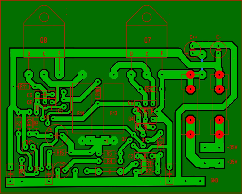
Take the post1858 layout as an example.
+ve current passes into +ve 35V terminal - +fuse holder - Q7e - Q7c - around the thick trace to top end of R13 - along R13 - common trace between the two resistors.
Where is the remainder of the current route to the speaker?
Where is the Return route from the speaker? It should be between the two resistors labelled R13 & R14, then follow the +ve current route described above, back to a terminal between +35V & -35V .
Last edited:
the power feed usesthree conductors. The current runs around two of these traces/wires. The third wire in the group is the Power Zero Volts.
It must be included in the LOW LOOP AREA layout design.
Simply closing up the +ve and -ve traces does not achieve low loop area if the Zero Volts is run to some remote star.
This sounds like an excellent way to induce a lot of noise into a ground.
- Status
- This old topic is closed. If you want to reopen this topic, contact a moderator using the "Report Post" button.
- Home
- Amplifiers
- Solid State
- Dx Blame ST - Builder's thread - post pictures, reviews and comments here please.