I'd check the values of R28 to R31.Everything measures near spec on the ltp. Vas. And both ccs. The only strange measurements are on the bases of the drivers... one measures 1.5v and the other -1.2v... off course that reflects also in the gates of the output mosfets that are also not simetrical
these voltages are nearly symmetrical.Everything measures near spec on the ltp. Vas. And both ccs. The only strange measurements are on the bases of the drivers... one measures 1.5v and the other -1.2v... off course that reflects also in the gates of the output mosfets that are also not simetrical
Had you measured +1.5V and +1.2V you had a problem.
Similarly -1.5V and -1.2V would indicate a problem.
Looks like up to the drivers is OK.
What are the Driver Vbe and the output Vgs.
If you have 0.3V at the output, then the gate input at the -IN node must also be pretty far from what exists at the +IN node.
What is the voltage drop across the two feedback resistors?
It is the jfet input ltp that uses very well matched lsk devices
when the offset adjustment is not enough..
you can set it back to mid span...
then you can adjust the settings on the small ccs...
R7 pot to see if you can trim it to 100mV......
when adjusting the R7 and you see no change,
that means you have a mistake somewhere...
if you are able to set that to 100mV with R7,
then use R17 to get that offset closer to 0 volts....
I'd check the values of R28 to R31.
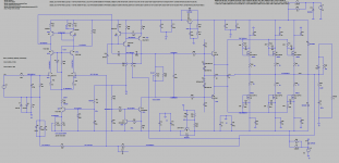
I am not using a vbe multiplier. my outputs are laterals so I use a resistor instead VR1 and R55 in my schematic in attach
Will measure those and report.... but the voltages at the gates of the laterals are not simetrical...these voltages are nearly symmetrical.
Had you measured +1.5V and +1.2V you had a problem.
Similarly -1.5V and -1.2V would indicate a problem.
Looks like up to the drivers is OK.
What are the Driver Vbe and the output Vgs.
If you have 0.3V at the output, then the gate input at the -IN node must also be pretty far from what exists at the +IN node.
What is the voltage drop across the two feedback resistors?
when the offset adjustment is not enough..
you can set it back to mid span...
then you can adjust the settings on the small ccs...
R7 pot to see if you can trim it to 100mV......
when adjusting the R7 and you see no change,
that means you have a mistake somewhere...
if you are able to set that to 100mV with R7,
then use R17 to get that offset closer to 0 volts....
In my schematic the offset is controled by vr2 on top of the mirror .... I can set it to have 4mA on both source resistors of the input LSK but that does not change offset...
The amp works ok in the bench producing nice sinewaves without crossover distortion but the 0.3v offset is disturbing...
Attachments
When I first built it with MJE for drivers it oscilated so I replaced the drivers with BD139 140 and placed small caps (15p) between gate and drain of the laterals.... also increased gate resistors to 220ohm and now it works ok... apart from the offset.
Is it possible that the offset results from not so near matching between negative and positive drivers / laterals ?
Is it possible that the offset results from not so near matching between negative and positive drivers / laterals ?
Is it possible that the offset results from not so near matching between negative and positive drivers / laterals ?
in my own experience, drivers were never a problem...
output voltage offset is a function of the entire circuit, not just individual components...
In my schematic the offset is controled by vr2 on top of the mirror .... I can set it to have 4mA on both source resistors of the input LSK but that does not change offset...
The amp works ok in the bench producing nice sinewaves without crossover distortion but the 0.3v offset is disturbing...
VR2 is not the best practice imho.....i will leave that as fixed 100ohm 1% resistors...
you can use the ltp current adjustment pots to trim off the output offset, VR3 in your schematic....
i can see another way of killing that output offset,
but i believe that adjusting tail currents will do the job.....
there is a world of difference between simulations and actual circuit conditions....
btw, is that offset positive or negative 300mV?
if positive, then decrease tail current, or vice versa...
the Nch currents should add up to exactly the same as the Pch currents.M1 204mA Nmos
M3 193mA Nmos
M4 214mA Pmos
M6 198mA Pmos
Ngate 0.88v
Pgate -0.75V
But they don't. You have an apparent 412mA Pch and 397mA, error ~3.8%
Did you select your source resistors to better than 1% (±0.5%)
All your measurments so far do not explain the 0.3V output offset error.
Are the input transistors passing the same drain current?
What is the Vdiff across the two source nodes?
What is the Vdiff across the two gate nodes? Measure to the outside of the gate resistors. Measuring directly to the gates may cause oscillation.
Agh !, there are no gate resistors !. Monitor the output with a scope to check as you touch the gates with a probe.
Last edited:
in my own experience, drivers were never a problem...
output voltage offset is a function of the entire circuit, not just individual components...
VR2 is not the best practice imho.....i will leave that as fixed 100ohm 1% resistors...
you can use the ltp current adjustment pots to trim off the output offset, VR3 in your schematic....
i can see another way of killing that output offset,
but i believe that adjusting tail currents will do the job.....
there is a world of difference between simulations and actual circuit conditions....
btw, is that offset positive or negative 300mV?
if positive, then decrease tail current, or vice versa...
What other way did you have in mind ? Servo ?
the Nch currents should add up to exactly the same as the Pch currents.
But they don't. You have an apparent 412mA Pch and 397mA, error ~3.8%
Did you select your source resistors to better than 1% (±0.5%)
All your measurments so far do not explain the 0.3V output offset error.
Are the input transistors passing the same drain current?
What is the Vdiff across the two source nodes?
What is the Vdiff across the two gate nodes? Measure to the outside of the gate resistors. Measuring directly to the gates may cause oscillation.
Agh !, there are no gate resistors !. Monitor the output with a scope to check as you touch the gates with a probe.
Thank you Andrew.
Do not have equipment sensible enough to measure correctly 0.1 resistors so I did not match those vishay wirewound 5W 0.1ohm 1%
I can dial Vdiff across the input sources to zero with VR2 so they pass 4mA each but that does nothing to the output offset.
Yesterday I tryed to measure Vdrop across the two feedback resistors and those are too small to measure correctly with my equipment.
I have described my method twice in the last year and more often before that.Thank you Andrew.
Do not have equipment sensible enough to measure correctly 0.1 resistors so I did not match those vishay wirewound 5W 0.1ohm 1%
You don't need sophisticated equipment to compare measurements of low value resistors. A DMM that reads 199.9mVdc, a current source that puts out a constant switched or adjustable 100mA to 200mA and some insulated terminals strips, or just solder the resistors together.
http://www.diyaudio.com/forums/soli...honey-badger-build-thread-62.html#post4127686
http://www.diyaudio.com/forums/soli...honey-badger-build-thread-62.html#post4128758
http://www.diyaudio.com/forums/soli...honey-badger-build-thread-62.html#post4129715
All the information is already in the Forum.
If you are measuring 0.3Vdc output offset, there must be voltages across the feedback resistors and across the Rin resistor.I can dial Vdiff across the input sources to zero with VR2 so they pass 4mA each but that does nothing to the output offset.
Yesterday I tryed to measure Vdrop across the two feedback resistors and those are too small to measure correctly with my equipment.
Note the bottom of Rin must be at zero volts ref signal return.
Output offset must be at 300.0mVdc ref signal return plus a correction for the DC Vdrop across the V ref link from signal return to speaker return.
Last edited:
post2 R3 = Rin. the resistor that sets the input impedance.
The input is AC coupled so shorting the input does not change the DC operating conditions. Shorting the inputs changes the input impedance seen by the +IN node from 33k to 0k82, so noise of the 33k resistor does not get amplified. This changes the AC voltage at the input and thus changes the AC voltage at the output.
Do not connect an output load when measuring the output offset.
output offset should not change when you short the input on the other side of that DC blocking capacitor.
Do you have C1 fitted? Is it a leaky electro, or a plastic film?
Last edited:
I am using jfet input (your LSK) so I do not need an input cap.
Please refer to the schematic on post 1644.
I believe that is why I have so low currents on the feedback resistors without signal on the input.
I am now building a second board to see if the problem persists.
Do you believe I can use MJE drivers without fear of oscilation ? (The pins on the BD139 140 are inverted so building is awkward)
Do you want to try one of my boards ? It would be a great help if you could beta test....
there's your output offset.I am using jfet input (your LSK) so I do not need an input cap.
You are pulling the input offset to almost zero by shorting the input with a Source, or a dummy zero ohms plug.
You need a DC blocking capacitor to prevent the output offset going all over the shop whenever you change sources.
Think back to the conditions that an input jFET runs at.
When the Vgs = zero the Id is roughly equal to Idss, when the Vds is @ 10Vds and the Tj = 25°C.
Now run the jFET at a current lower than Idss and you find it needs a negative Vgs. Look athe datasheet plot to see how much the Vgs grows as the Id is reduced.
If you run the Id @ ~50% Idss you will find that ~0.1Vgs to 0.5Vgs (depending on the device Idss) is generated. Because you are NOT operating at Idss.
This Vgs is seen as an input offset.
Look at opamp specifications and similar to chipamps, they all quote an input offset.
The jFET input LTP is the same.
Last edited:
- Home
- Amplifiers
- Solid State
- diyAB Amp - The "Honey Badger"