I finally got it going with the LTSpice. It was my fault.........I've been spending a lot of time on this the last few days, the simulation is so so slow. Just made a stupid mistake.
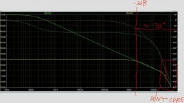
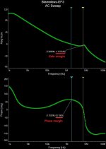
Anyway, I think I was right, the simple circuit is stable from my understanding on the simulation on the open and closed loop gain phase plot. I attached the new file with two identical circuits, one with closed loop gain of 21( the right). I change R33 on the left circuit from 1K to 0.1ohm ( in the feedback gain setting) to simulate openloop gain. I plot the gain and phase plot of both the open loop ( green) and closed loop (yellow/light grey).
You can see it's a single pole roll off from about 100Hz to about 5MHz before going to 2 poll roll off and the phase gone south. BUT we have a gain of 21, at the -3dB point of the amplifier ( vertical red line labeled -3dB), the phase shift is only -70deg. I have 180-70=110deg phase margin. The phase at 0dB is irrelevant as circled "Don't care".
The circuit should be stable. But then again, this is on paper/computer. Real circuit might be different.
Hi MiiB,
I try to look for Tien probe, I don't quite follow. But I think the way I make R33 to 0.1ohm should work close enough. When I search for Tien probe, I saw description using Spice derivitives which I don't understand. I am not very good with simulations.
Thanks
Attachments
Bear in mind that looking at in-situ distortion of the output stage by connecting the analyzer to the center-tap of the driver does not require a balanced input.
Looking at the driver center-tap distortion of an output stage in-situ in a closed loop can be quite revealing of how much distortion the output stage is contributing open-loop. the number -30 dB (about 3% HD) does sound a bit bad, however.
Traditional crossover distortion is basically static, and largely independent of frequency in the open loop. In the closed loop, it will go up with frequency because the feedback loop gain is going down with frequency. So, for evaluation of ordinary non-frequency-dependent crossover distortion in an output stage, just taking a look at 1kHz THD is a very good start.
Cheers,
Bob
Hi Bob
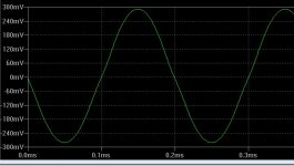
The distortion is really that bad, I did simulation a few times to verify. I attached the .asc where I label the two points I probed and the waveform plot of the probe. You can see the distortion.
But if you look at my other post with the complete amp, it's just a simple power amp design like the Blameless from Doug Self with the ideas from your book on 300ohm emitter resistor on the LTP, CM load of the LTP and darlington VAS and with 3EF. The distortion is amazingly low. The feedback got rid of most of the distortion.
Seems like a good simple clean design is very good already. Increasing the open loop gain ( using the above described in your book) is very effective in lowering the distortion.
I like to hear your opinion.
Attachments
We need to bear in mind that there are two ways of looking at the output stage distortion when using a center-tapped driver.
The first one is to take the feedback from the center tap and measure the distortion at the output of the amplifier; in this arrangement, the output stage is outside the feedback loop, and we assume that the amplifier creates much lower distortion when the loop is closed from the driver center tap. In this arrangement, we are essentially trying to drive the output stage with a low-distortion, low-impedance source (the output of the driver).
The second one is the one I suggested and prefer. In the second arrangement, the feedback loop is still closed from the output of the output stage and the topology of the amplifier is left undisturbed. We then just look at the center tap of the driver with a high-impedance load (the analyzer). We are measuring with the output stage in-situ, inside the feedback loop. In this case, we are looking at the distortion that the output stage must be driven with to undo its distortion contribution. We are looking at inverse distortion, whose amplitudes will be about the same as the true distortion, even though the waveform of the distortion products at this node is inverted.
Cheers,
Bob
Hi Bob,
NOW I see what you mean (2-nd option). Very clever approach - thanks a lot for sharing.
Cheers,
Valery
Use the Tian probe method from the exsaples directory of LT-spice, that will give you a good indication of circuit stability. A dirty an quick glanze can be made by breaking the loop with a 1GH inductor.
Care must be taken in using the Tian probe to avoid inadvertent mistakes. When possible (which is most of the time), the breaking of the global loop with a large inductor should be used as a sanity check. Indeed, for most ordinary amplifiers, bidirectional signal flow and loading in the feedback loop where the loop is broken is very small and can be ignored. These probes are most important when breaking the loop disturbs the topology in such a way that circuit operation is significantly changed.
This will often be the case when both sides of the breakage point have significant impedance effects on the other side; i.e., bidirectional interaction. For example, if the source side and the load side of the breakage point have impedance on the same order of magnitude, breaking the loop at that point with an inductor will yield inaccurate results.
If an amplifier has several loops internal to the global NFB loop, and one wants to look at the total loop gain enclosing a particular piece of circuitry, these type probes can be important, as it is hard to break the loop with an inductor without disturbing circuit operation.
For looking at the loop gain, gain margin and phase margin of the global loop of a reasonably conventional power amplifier, breaking the loop with an inductor, while seemingly crude, yields pretty good results.
Also, simulating the amplifier with much higher closed loop gain, thereby "exposing" the open loop behavior, can also yield good insight.
Finally, some good test techniques, either in simulation or on real amplifiers, include halving the closed loop gain (doubling the loop gain) to see if the amplifier is still stable (quick check for gain margin >6dB) and placing an added pole in the feedback network at a frequency near ULGF (quick test for phase margin). I often build an amplifier with the feedback resistor made up of two equal-value resistors in series. With access to the feedback resistor center tap thereby created, doing these quick checks is easy. This approach also cuts in half the dissipation in the FB resistor.
It is also worthwhile to check the amplifier for conditional stability gain margin by doubling the closed loop gain by, say 6dB (cutting loop gain by 6dB). Some amplifiers using TPC compensation may go unstable under these conditions.
Cheers,
Bob
Thanks Bob.. i have made a design with only one gain-stage, this mean that i close the loop arround very little capacitance an thus I have really good gain an phasemargien (close to 90 degrees at 0 dB gain. When the loop is closed. Apart from the low frequency peak you always when you break with large inductor, both the tian and inductor method give very close to the same result.
For output stage I have made a two tier system where an array of 8 or 16 set of bipolar s deliver the current and a set of laterals biased with 140mA sets the spread to the signal, this way you can actually avoid any switching if load stays above 2ohm nominal.
For output stage I have made a two tier system where an array of 8 or 16 set of bipolar s deliver the current and a set of laterals biased with 140mA sets the spread to the signal, this way you can actually avoid any switching if load stays above 2ohm nominal.
Care must be taken in using the Tian probe to avoid inadvertent mistakes. When possible (which is most of the time), the breaking of the global loop with a large inductor should be used as a sanity check. Indeed, for most ordinary amplifiers, bidirectional signal flow and loading in the feedback loop where the loop is broken is very small and can be ignored. These probes are most important when breaking the loop disturbs the topology in such a way that circuit operation is significantly changed.....................
Also, simulating the amplifier with much higher closed loop gain, thereby "exposing" the open loop behavior, can also yield good insight............
Cheers,
Bob
I don't quite understand Tien probe, something borders me about adding a voltage source to break the loop.
As you can see in my post #161, I use 0.1ohm resistor in the feed back to make closed loop gain of 20K/0.1= 200000. essentially making it open loop gain to look at the phase margin when at -3dB point of the amplifier(2MHz).
Unfortunately, the way it is shown, it will not work in the real world.
102db loop gain at 1KHz (huge), only 4db gain margin (almost none).
Meaning - it's unstable. Even in simulation - if you send it into clipping (which is rather awful - full of artifacts), it starts oscillating on recovery.
102db loop gain is rather difficult to stabilize. Possible, but you will have to sacrifice many other good things. Not worth it.
Feedback loop analysis of your circuit is attached.
Hi Valery
I kept looking at this post. I don't know why your simulation looks a little different from mine using LTSpice. you have a slight peak at about 10MHz and LTSpice does not have that. LTSpice just show -40dB roll off at about 20MHz.
But even if you look at your simulation, if you draw a horizontal line of about 26dB to represent the closed loop gain of 21, the line will intersect at a point you have a lot more gain phase margin. We only look at the -3dB point of the amplifier gain, not at the 0dB point of the open loop gain.
Let me know what you think.
Thanks
I may be misunderstanding you, but phase margin is defined by the phase at the frequency where the loop gain goes through 0dB (also called the gain crossover frequency).
The closed loop -3dB frequency will almost always be at a somewhat higher frequency because the phase margin is usually somewhat less than 90 degrees. The closed loop frequency response -3 dB frequency is thus enhanced somewhat by the departure of the phase margin from 0 degrees.
Cheers,
Bob
Yes, phase margin is defined at the freq where loop gain=0. If the closed loop gain is 21, the phase margin is defined where the open loop gain curve intersect the close loop gain line( at about 27dB).
If you look at the plot in post #161, I showed exactly that with markers on. I think my simple amplifier is unconditionally stable.
Can you verify that I am correct?
Thanks
Last edited:
When you lover the impedance of the feedback network you also alter the phase gain plots. Your method is non valid one wil not correlate with reality in any way. Your phase turns too much for the amplifier to be stable, I wil oscillate at a few MHz
The inductor method is better
The inductor method is better
When you lover the impedance of the feedback network you also alter the phase gain plots. Your method is non valid one wil not correlate with reality in any way. Your phase turns too much for the amplifier to be stable, I wil oscillate at a few MHz
The inductor method is better
I think you are referring to the pole formed by the feedback network impedance and the effective input capacitance of the input stage. If this pole is significant in terms of adding lagging phase shift, it will indeed be pushed to a higher frequency when closed loop gain is increased by decreasing the resistance value of the feedback network shunt resistor. However, if for no other reason than noise, the shunt feedback resistor should usually be on the order of 1k or less (thermal noise of a 1k resistor is about 4 nV/rt Hz). I usually choose a shunt resistor value of about 500 ohms. This keeps the feedback node pole at a reasonably high frequency (500 ohms and even 10pF creates a pole at 32 MHz, pretty far above a typical gain crossover frequency of 1 MHz).
Nevertheless, if one wants to increase closed loop gain for evaluation purposes, it is better to do it by increasing the value of the series feedback resistor, or center-tapping it and add an intermediate shunt to ground.
The inductor method is fine in simulation, but impractical for implementation in the real world on a prototype amplifier.
Cheers,
Bob
When you lover the impedance of the feedback network you also alter the phase gain plots. Your method is non valid one wil not correlate with reality in any way. Your phase turns too much for the amplifier to be stable, I wil oscillate at a few MHz
The inductor method is better
I tried the inductor with very high inductance, it does not show a good plot, it peaked at some strange frequency.
It's not exactly my design, rather just a typical circuit from text book by Doug and Bob. I am sure they can answer in more detail as they all have circuit like this.
I experimented with different value caps, the phase shift is just as much. If this circuit is not stable, then they have to revise their books too.
Last edited:
I think you are referring to the pole formed by the feedback network impedance and the effective input capacitance of the input stage. If this pole is significant in terms of adding lagging phase shift, it will indeed be pushed to a higher frequency when closed loop gain is increased by decreasing the resistance value of the feedback network shunt resistor. However, if for no other reason than noise, the shunt feedback resistor should usually be on the order of 1k or less (thermal noise of a 1k resistor is about 4 nV/rt Hz). I usually choose a shunt resistor value of about 500 ohms. This keeps the feedback node pole at a reasonably high frequency (500 ohms and even 10pF creates a pole at 32 MHz, pretty far above a typical gain crossover frequency of 1 MHz).
Nevertheless, if one wants to increase closed loop gain for evaluation purposes, it is better to do it by increasing the value of the series feedback resistor, or center-tapping it and add an intermediate shunt to ground.
The inductor method is fine in simulation, but impractical for implementation in the real world on a prototype amplifier.
Cheers,
Bob
Hi Mr. Cordell
What I have is just a very simple amplifier circuit using the suggestions in your book. The 300ohm emitter resistor for LTP to linearize the LTP. Current mirror load to get back the loss of gain by the 300ohm emitter resistors. Using darlington VAS to avoid loading the LTP stage. That's it. You use same compensation like my circuit as I copy from you.
As for extra pole at the -ve input that is masked by low value shunt resistor, it's easy to fix just by a small feedback cap across the feedback resistor.
I think it's better if you answer MiiB and Valery's concern. I don't want to pretend to be an expert.
Thanks
Last edited:
Hi Valery
I kept looking at this post. I don't know why your simulation looks a little different from mine using LTSpice. you have a slight peak at about 10MHz and LTSpice does not have that. LTSpice just show -40dB roll off at about 20MHz.
But even if you look at your simulation, if you draw a horizontal line of about 26dB to represent the closed loop gain of 21, the line will intersect at a point you have a lot more gain phase margin. We only look at the -3dB point of the amplifier gain, not at the 0dB point of the open loop gain.
Let me know what you think.
Thanks
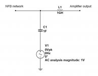
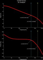
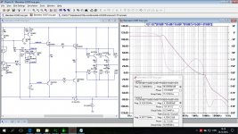
The difference is because I'm looking "inside the loop". One of the simple methods of analyzing the feedback loop (including stability margins assessment) was described by Bob Cordell long time ago. See the attached diagram. The amp's input is grounded. The AC signal source is injected into the feedback path, being isolated the right way with huge capacitor and inductor - advantage of simulators, GigaHenry is no problem.
In this case, you see the magnitude and phase responses vs frequency of the feedback loop. You can see ULGF, phase and gain margins, poles and zeroes of the feedback system. Tian probe is more sophisticated, but this simple method is accurate enough, at least for me.
I attach your loop analysis again (green) along with a stable one (red) for a reference.
Attachments
Here is the Loop Gain simulated with Tian probe, PM=62 dB, GM= 4 degree. I changed some models as I don't have them.
You have to work on it a bit more.
Pretty close to what I've got with simple method

Hi Valery
Thanks for the reply, I need time to think and try the simulation again. I am quite new at this, everything is from the books. I trust you have the real life experience.
I am slow, I have been spending a lot of time on this. Let me stew on this first!!!! Like Terminator said "I'll be back"!!!
Thanks for the reply, I need time to think and try the simulation again. I am quite new at this, everything is from the books. I trust you have the real life experience.
I am slow, I have been spending a lot of time on this. Let me stew on this first!!!! Like Terminator said "I'll be back"!!!
Here is the Loop Gain simulated with Tian probe, PM=62 dB, GM= 4 degree. I changed some models as I don't have them.
You have to work on it a bit more.
Hi Dadod
Sorry some how I missed your post until Valery mentioned this.
I just simulated, it looked strange. Can you explain how does this work? You have a voltage and a current generator.
I have to read the new stuffs you added like the image attached. I never get this advanced.
Thanks
Attachments
- Status
- This old topic is closed. If you want to reopen this topic, contact a moderator using the "Report Post" button.
- Home
- Amplifiers
- Solid State
- New Class A, Super-A, Non-Switching : need a revival ?