well, yes!
Same as most of the other OPS configurations - two CCSs 5mA each (one with a trimmer for setting the offset to zero), 2 capacitors between the input and the pre-drivers' bases (the top and the bottom of the bias spreader).
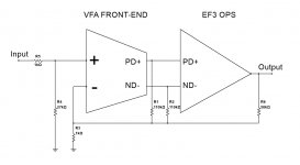
However, I like the attached configuration much better (I worked on it about a year ago), comparing to the one with the OPS being completely out of GNFB loop. You can control the amount of NFB covering the OPS, adjusting the ratio between the R1||R2 and R6.
Attachments
Here is the way I do it. I measure or simulate the output stage distortion in-situ, with the complete amplifier in place. This takes a lot of guesswork out of the process.
Whenever I build and amplifier, I center-tap the driver emitter bias resistor that connects the emitters of the top and bottom drivers. This node is basically the input to the output stage. With feedback in place, total amplifier distortion is much lower than the open-loop distortion of the output stage up to frequencies well above 20kHz. If you place a distortion analyzer at this center-tapped driver node, you will see the distortion that is needed to drive the output stage to make a low-distortion output.
This is just input-referred distortion of the output stage. Its absolute polarity is inverted, but this does not matter. This approach to evaluating output stage distortion is valid as long as the amplifier output distortion is at least, say, 10 times less than the open-loop distortion of the output stage.
Cheers,
Bob
Thanks Bob
I don't have a distortion analyzer, what is a good enough, reasonable price one?
Last edited:
Thanks Bob
I don't have a distortion analyzer, what is a good enough, reasonable price one?
You might check on Ebay for a used Audio Precision AP-1 or an HP 339A. Also, sometimes a Tek TM500 AA501 becomes available. It does not include a source oscillator, so you will also need an SG505 to go with it.
But some PC-based solutions that use soundcards or the Quantasylum device may also serve you needs.
Cheers,
Bob
Bob - a good one, as long as we don't consider the pre-drivers being part of the OPS.
When I ran initial tests on the non-switching prototype, I have split the NFB resistor into 2 x double-value ones and connected them to the positive and negative shoulders of push-pull VAS output (just on both sides of bias spreader) - works well if NFB netwok's impedance is relatively high.
The drawback of the approach - we slightly load the VAS, decreasing its output impedance at the same time (improving its driving capabilities with regards to OPS). However, the whole OPS, including the pre-drivers, is running clean outside the global loop, allowing open loop measurements and valid comparison with other OPS topology options.
Cheers,
Valery
As long as the drivers in a 3EF output stage remain in control of the output transistors (i.e., adequate bias current so they do not turn off when trying to turn off the output transistor), they should contribute far less distortion than the class AB output stage (assuming drivers always operate in class A, as in a Locanthi Triple). Obviously, in a Triple, one can also look at the center tap of the pre-driver emitter bias resistor.
Cheers,
Bob
You might check on Ebay for a used Audio Precision AP-1 or an HP 339A. Also, sometimes a Tek TM500 AA501 becomes available. It does not include a source oscillator, so you will also need an SG505 to go with it.
But some PC-based solutions that use soundcards or the Quantasylum device may also serve you needs.
Cheers,
Bob
Thanks Bob
I actually have the QuantAsylum. But it won't work the way you suggested as it is a single end input where one side is grounded.
I have been doing simulation with LTSpice with your idea of tapping the middle of the resistor between the two driver transistors. I even put a voltage divider across the voltage spreader ( using 1M resistor for divider so not to load the VAS). The result is bad!!! I did two or three OPS even with crossover compensation and I did not get better than -30dB on the more important 3rd harmonic. I even ran the simulation of the famous Nelson Pass's Aleph3 ( that actually got me looking into all these crossover compensation) and the result is not that good.
I want your opinion whether I am right or not: if I run the usual 1KHz, 5KHz, 10KHz and 20KHz FFT. More importantly, run two tone test at say 10KHz. Pick the one that is lowest and go with it. If I get over -90dB on the harmonics or intermod, that's a good design whether there is crossover compensation or not.
I don't know how to simulate TIM distortion test.
I am reading your book on the MOSFET output stage. I am still trying to figure how to find the optimal value of the source resistor to minimize crossover distortion. That is I want to get some formula or guideline to pick the value using the transconductance graph of the MOSFET.
Thanks
Last edited:
As long as the drivers in a 3EF output stage remain in control of the output transistors (i.e., adequate bias current so they do not turn off when trying to turn off the output transistor), they should contribute far less distortion than the class AB output stage (assuming drivers always operate in class A, as in a Locanthi Triple). Obviously, in a Triple, one can also look at the center tap of the pre-driver emitter bias resistor.
Cheers,
Bob
In simulation, I tried exactly what you suggested AND I put a voltage divider across the bias spreader to tape the mid point. Result is exactly the same. I was expecting to get more distortion when tapping the bias spreader as it includes the change of Vbe of the drivers...or pre-drivers for 3EF. But it's exactly the same.
In simulation, I tried exactly what you suggested AND I put a voltage divider across the bias spreader to tape the mid point. Result is exactly the same. I was expecting to get more distortion when tapping the bias spreader as it includes the change of Vbe of the drivers...or pre-drivers for 3EF. But it's exactly the same.
Well, depends on the values you are using for the divider.
Are you sure your output stage is optimally biased?
Optimal bias threshold is rather narrow, so adding a divider in parallel with the spreader would definitely influence the bias, if the R values are rather low.
Ah! I see now - it's 1M - then it's too high.
Anyway, it looks to me that the bias is not optimal in your simulations. Too consistently high, from what I see.
Last edited:
Well, depends on the values you are using for the divider.
Are you sure your output stage is optimally biased?
Optimal bias threshold is rather narrow, so adding a divider in parallel with the spreader would definitely influence the bias, if the R values are rather low.
Ah! I see now - it's 1M - then it's too high.
Anyway, it looks to me that the bias is not optimal in your simulations. Too consistently high, from what I see.
One thing good about in simulation, you don't worry about parasitic capacitance. I verified, the "e" source I use to buffer the divider has infinite input impedance. It is perfectly ok using 1M resistor in simulation( not a chance in real world). I got identical result with the suggestion of taping the resistor of the driver stage as Bob suggested.
I carefully adjust the current close to 100mA per output transistor pair and use 0.25ohm emitter resistor for optimal bias.
That is not to say it does not have good result in real world. But I am only starting to investigate into this crossover cancellation idea, you have real world experience and spent over a year on it already. For all I know, I might be doing something wrong in the simulation.
I am just trying to understanding more on this subject. Simulation is the cheapest way to do it!!!
Audiocrase.
A mosFET output stage does not have an optimal bias voltage/current.
It is different from a BJT output stage.
The EF form of the BJT output stage has an optimal bias voltage of ~26mV when around room temperature. This rises proportionally with difference above absolute zero, i.e. K
eg. if bias voltage = 26mV at 300K, then at 330K the bias voltage required has increased to 330/300*26 = 28.6Vbias.
MosFETs just get less crossover distortion as you raise the bias current. And keep going until you reach ClassA where crossover distortion has dropped to zero.
One thing good about in simulation, you don't worry about parasitic capacitance. I verified, the "e" source I use to buffer the divider has infinite input impedance. It is perfectly ok using 1M resistor in simulation( not a chance in real world). I got identical result with the suggestion of taping the resistor of the driver stage as Bob suggested.
I carefully adjust the current close to 100mA per output transistor pair and use 0.25ohm emitter resistor for optimal bias.
That is not to say it does not have good result in real world. But I am only starting to investigate into this crossover cancellation idea, you have real world experience and spent over a year on it already. For all I know, I might be doing something wrong in the simulation.
I am just trying to understanding more on this subject. Simulation is the cheapest way to do it!!!
It is assumed, that you connect NFB resistor to the center tap of the emitter resistor (in case of the pre-drivers approach, as Bob recommended), or you connect it to the center tap of the divider, placed over the spreader (in case of VAS approach, as I described earlier).
Now, if this divider, placed over the spreader, is made of 1M resistors, your NFB loop gain is changed significantly (to almost open loop). That's why this is not the right way of doing it. That's why I split the NFB resistor in 2, double the value of each of them, and connect them on both sides of the spreader. Then the loop gain stays the same for the front-end.
Hi
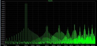
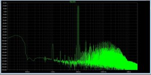
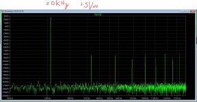
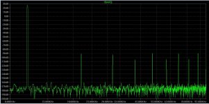
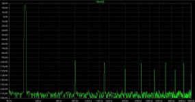
Since I have no luck with simulation, so I turn to the opposite direction. I have been playing around with simulation of a simple minded "Blameless" something like Doug Self used with 3EF and 3 pairs of output transistors at optimal bias. I only posted the one with 30V output for 1, 5, 10 and 20KHz. I include also two 2Tone simulation of 10KHz and 20KHz center frequency. You can see the harmonics are over 100dB down from the main signal. The 2 Tone simulations look very good with over 100dB. I also attached the .asc I used to generate these plots.
I don't know how representative are the simulation to the real circuit, whether you can get these result in real life. But over 100dB in every single case, 120dB at lower signal level like 10V output. That's pretty impressive. Particularly I use 4ohm load, not 8 ohm.
Attachments
-
 Two tone Blameless 3EF X3pairs 19.5KHz 20.5KHz 0.75V.JPG177.3 KB · Views: 91
 -
 Two tone Blameless 3EF X3pairs 9.5KHz 10.5KHz 0.75V.JPG225 KB · Views: 394
 -
 Blameless 3EF X3pairs20KHz 1.5V.JPG215 KB · Views: 409
 -
 Blameless 3EF X3pairs 10KHz 1.5V.JPG192.8 KB · Views: 406
 -
 Blameless 3EF X3pairs 5KHz 1.5V.JPG163 KB · Views: 416
 -
 Blameless 3EF X3pairs 1KHz 1.5V.JPG130.6 KB · Views: 428
 -
Blameless 3X3EF.asc11.7 KB · Views: 84
Last edited:
Hi
Since I have no luck with simulation, so I turn to the opposite direction. I have been playing around with simulation of a simple minded "Blameless" something like Doug Self used with 3EF and 3 pairs of output transistors at optimal bias. I only posted the one with 30V output for 1, 5, 10 and 20KHz. I include also two 2Tone simulation of 10KHz and 20KHz center frequency. You can see the harmonics are over 100dB down from the main signal. The 2 Tone simulations look very good with over 100dB. I also attached the .asc I used to generate these plots.
I don't know how representative are the simulation to the real circuit, whether you can get these result in real life. But over 100dB in every single case, 120dB at lower signal level like 10V output. That's pretty impressive. Particularly I use 4ohm load, not 8 ohm.
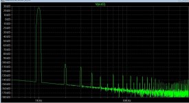
Unfortunately, the way it is shown, it will not work in the real world.
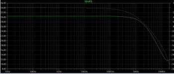
102db loop gain at 1KHz (huge), only 4db gain margin (almost none).
Meaning - it's unstable. Even in simulation - if you send it into clipping (which is rather awful - full of artifacts), it starts oscillating on recovery.
102db loop gain is rather difficult to stabilize. Possible, but you will have to sacrifice many other good things. Not worth it.
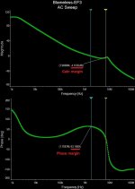
Feedback loop analysis of your circuit is attached.
Attachments
Unfortunately, the way it is shown, it will not work in the real world.
102db loop gain at 1KHz (huge), only 4db gain margin (almost none).
Meaning - it's unstable. Even in simulation - if you send it into clipping (which is rather awful - full of artifacts), it starts oscillating on recovery.
102db loop gain is rather difficult to stabilize. Possible, but you will have to sacrifice many other good things. Not worth it.
Feedback loop analysis of your circuit is attached.
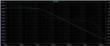
I ran the simulation on both close loop and open loop gain phase plot. Yes, it is not stable at the end of the plot. I ran the open loop by changing R123( feedback resistor) to 1ohm to increase the gain of the amp to 20000. This pretty much show the open loop gain to plot the gain phase.
I don't think it look that bad. From looking at the plot, it should be not that hard to put a lag lead at frequency beyond 20KHz(beyond audio range) to get a little more phase margin. Say putting a poll at 25KHz and a zero at 200KHz to drop about 20dB gain, I don't think it will increase the distortion much. But say it increase by 10dB. Still in most part, it's over 100dB down. I'll get to it when I have time.
I ran at output =30V into 4ohm. That's tough. If I run smaller signal, driving 8ohm, I likely will get about -110dB distortion even with extra compensation.
But again, this is theoretical talk.
Attachments
Last edited:
I ran the simulation on both close loop and open loop gain phase plot. Yes, it is not stable at the end of the plot. I ran the open loop by changing R123( feedback resistor) to 1ohm to increase the gain of the amp to 20000. This pretty much show the open loop gain to plot the gain phase.
I don't think it look that bad. From looking at the plot, it should be not that hard to put a lag lead at frequency beyond 20KHz(beyond audio range) to get a little more phase margin. I don't think it will increase the distortion much. But say it increase by 10dB. Still in most part, it's over 100dB down. I'll get to it when I have time.
I ran at output =30V into 4ohm. That's tough. If I run smaller signal, driving 8ohm, I likely will get about -110dB distortion even with extra compensation.
But again, this is theoretical talk.
You have to use one of the methods for looking what happens inside the loop when the loop is closed (that's what my plot shows).
Running it open loop does not give you the right picture.
Thanks Bob
I actually have the QuantAsylum. But it won't work the way you suggested as it is a single end input where one side is grounded.
I have been doing simulation with LTSpice with your idea of tapping the middle of the resistor between the two driver transistors. I even put a voltage divider across the voltage spreader ( using 1M resistor for divider so not to load the VAS). The result is bad!!! I did two or three OPS even with crossover compensation and I did not get better than -30dB on the more important 3rd harmonic. I even ran the simulation of the famous Nelson Pass's Aleph3 ( that actually got me looking into all these crossover compensation) and the result is not that good.
I want your opinion whether I am right or not: if I run the usual 1KHz, 5KHz, 10KHz and 20KHz FFT. More importantly, run two tone test at say 10KHz. Pick the one that is lowest and go with it. If I get over -90dB on the harmonics or intermod, that's a good design whether there is crossover compensation or not.
I don't know how to simulate TIM distortion test.
I am reading your book on the MOSFET output stage. I am still trying to figure how to find the optimal value of the source resistor to minimize crossover distortion. That is I want to get some formula or guideline to pick the value using the transconductance graph of the MOSFET.
Thanks
Bear in mind that looking at in-situ distortion of the output stage by connecting the analyzer to the center-tap of the driver does not require a balanced input.
Looking at the driver center-tap distortion of an output stage in-situ in a closed loop can be quite revealing of how much distortion the output stage is contributing open-loop. the number -30 dB (about 3% HD) does sound a bit bad, however.
Traditional crossover distortion is basically static, and largely independent of frequency in the open loop. In the closed loop, it will go up with frequency because the feedback loop gain is going down with frequency. So, for evaluation of ordinary non-frequency-dependent crossover distortion in an output stage, just taking a look at 1kHz THD is a very good start.
Cheers,
Bob
It is assumed, that you connect NFB resistor to the center tap of the emitter resistor (in case of the pre-drivers approach, as Bob recommended), or you connect it to the center tap of the divider, placed over the spreader (in case of VAS approach, as I described earlier).
Now, if this divider, placed over the spreader, is made of 1M resistors, your NFB loop gain is changed significantly (to almost open loop). That's why this is not the right way of doing it. That's why I split the NFB resistor in 2, double the value of each of them, and connect them on both sides of the spreader. Then the loop gain stays the same for the front-end.
We need to bear in mind that there are two ways of looking at the output stage distortion when using a center-tapped driver.
The first one is to take the feedback from the center tap and measure the distortion at the output of the amplifier; in this arrangement, the output stage is outside the feedback loop, and we assume that the amplifier creates much lower distortion when the loop is closed from the driver center tap. In this arrangement, we are essentially trying to drive the output stage with a low-distortion, low-impedance source (the output of the driver).
The second one is the one I suggested and prefer. In the second arrangement, the feedback loop is still closed from the output of the output stage and the topology of the amplifier is left undisturbed. We then just look at the center tap of the driver with a high-impedance load (the analyzer). We are measuring with the output stage in-situ, inside the feedback loop. In this case, we are looking at the distortion that the output stage must be driven with to undo its distortion contribution. We are looking at inverse distortion, whose amplitudes will be about the same as the true distortion, even though the waveform of the distortion products at this node is inverted.
Cheers,
Bob
- Status
- This old topic is closed. If you want to reopen this topic, contact a moderator using the "Report Post" button.
- Home
- Amplifiers
- Solid State
- New Class A, Super-A, Non-Switching : need a revival ?