Yes, I'm clear about that. However, I don't see them as big advantages.
We can easily get gain in the power stage with the addition of a pair of drivers. Even though I prefer to drive mosfets directly with the VAS, in this instance, I would rather have drivers because driving the power mosfets directly from the VAS requires quite a bit of "juice". If the VAS don't have enough current, the amp will slew limit early.
As for direct mounting, I have no issues with mica and thermal compound. I do agree that mounting is faster without insulators and there's slightly better heat transfer but I don't view it as a quantum gain.
Putting aside the PS, can you help me out on where the Positive feedback loop is? I simply can't seem to locate it.
Cheers
Mike
Michael Chua said:Hi Paul
....
Michael - you got it wrong ....... in previous post a, same as in this one , regarding 9505 ..
first - rails aren't +/- 35
second - there is no perpetuum mobile in that amp
third 9505 is behaving absolutely the same , that's same output ....
Hi Zen Mod
Yes, I was wrong. I can see they are +HV and -HV. Somehow, I saw them as +/-35V.
The rails are indeed much higher. As Paul pointed out, the P9505 is about +/- 84V. I took another look at the QSC1400 and their rails are at +/-75V. So the rails are at the same voltages as a conventional PS where 0V in the center of the PS.
I understand that in order to have Gain in the current stage, the mosfets are arranged as common source. Output will therefore be at Drain.
What I am saying is if we revert back to a conventional PS by shifting the 0V back to the center of the PS and adding a pair of drivers after the VAS, we can still get Gain in the output stage.
I don't know how much it will affect the voltage nodal point in Strickland's patent by doing this. What is clear in his patent is 3 feedback mechanism are employed. 2 are negative feedback and 1 is positive feedback. I still cannot find the positive feedback loop.
There is one other point that I am puzzled. In the P9505, there are only 4 pairs of lateral mosfets. I assume they are 2SK1058 and 2SJ162 running at +/-84V rails. Is this not a bit too demanding on the mosfets?
Cheers
Mike
Michael Chua said:Hi Zen Mod.....
Cheers
Mike
as I see it , there are at least 3 important things :
1 . all mentioned amps ( Haflers) have that TransNova output config , but I can't see in any of them error correction implemented in Patent
2.you can - if you want - re-arrange almost any "conventional" amp to this sort of output/PSU , same as you can re-arrange Hafler to conventional output/PSU config.
3. is it Hafler output common drain , or common source - that's completely another issue , without special connection to TransNova output/PSU config ........ or I'm misiing something ?
maybe , because I really need to spend some more time on patent reading ....
you can see different output configurations ( common drain, common source ) in Papa's amps .... each of them have own virtues ...
anyway - regarding number of output mosfets .... Hafler was always even conservative in power ratings of their amps
even if these mosfets are ratyed for Uds of 160V , I suspect that they can see full throttle PSU voltage ever
some info from manual of 9303/9505
THEORY AND OPERATION OF transïnova
The (TRANSconductance NOdal Voltage Amplifier) principle is based on our 1984 U.S. Patent 4,467,288. This patent
describes the advantages of audio power amplifiers in which a MOSFET output stage is connected in a grounded source
configuration. In this connection the output stage has its full voltage gain of typically 20dB (ten times), instead of the
usual 1dB loss of voltage follower designs.
It is an inevitable result of electrical physics that this output with gain inherently increases the power gain (for the same
bandwidth) of the output stage by typically ten times over the conventional follower connection, using exactly the same
MOSFET devices.
The output stage is thus now ten times less wasteful of its incoming drive power. The driver stage can now be of a low
voltage (±24 volts) nature and be designed along the same principles always used in high quality preamplifiers: Class
A operation, high linearity, and wide bandwidth. A topology utilizing an output stage with gain yields a much simpler,
shorter total signal path than that of the usual high voltage driver designs. The number of serial stages is reduced from
five or more, to only three.
But all of the above does not make an amplifier transï
nova. The output stage is further refined into a trans-impedance
stage (current-to-voltage converter), to achieve extremely short loop (fast) negative feedback. The output stage is driven
cooperatively by a transconductance stage (voltage-to-current converter).
nova principle.
The 9303and 9505are the most sophisticated amplifiers we have yet developed utilizing the basic transï
And, although the measured specifications are very good, the numbers do not describe the realistic sound of the
amplifiers.
CIRCUIT IMPLEMENTATION
Earlier models of amplifiers we have offered using the transïnova topology have earned the reputation for clean, natural
sounding reproduction. A conservative, purist design approach was used to avoid compromising the desirable
characteristics of the transïnova circuits. Circuit innovation was not prevented by this conservatism; as is evident in the
discoveries which resulted in development of the DIABLO circuitry to be discussed shortly, and the novel balanced input
system.
Many ìbalancedî amplifiers are merely conventional unbalanced designs with a Balanced-to-Unbalanced converter
(usually IC op-amp based) preceding the power amplifier. The 9303 and 9505, however, are true differential input power
amplifiers. Each (+) and (ñ) input port has been buffered to allow direct signal access to the differential amplifier, without
conversion to unbalanced form. Deactivating the Balanced Mode is accomplished via a rear panel switch that grounds
the (ñ) inputs, effectively converting the amplifier to unbalanced operation.
The input stage is a JFET differential amplifier. This circuit configuration results in excellent front end headroom and
extremely low intermodulation effects. The ultra low noise characteristic of the JFETs virtually eliminates noise ìmixingî
(intermodulation) with the music signal, reducing discordant product frequencies known as ìnoise grainî or ìnoise
fuzz.î A servo integrator has been employed to establish minimal DC offset. This circuit monitors the DC offset at the
output of the amplifier, and injects an equal but opposite DC voltage into the (+) port of the differential input, thereby
cancelling the offset. This method eliminates the need for a sonically degrading electrolytic capacitor in the audio path,
and provides superior subsonic frequency response.
The final output stage utilizes lateral MOSFETs; four pairs are used for each channel in the 9505 and three pairs in the
9303. These devices, unlike conventional bipolar transistors do not exhibit ìthermal runaway.î Thermal runaway is a
phenomenon whereby a transistor heats up as it draws more current, which causes it to get hotter, and conduct more
current, and so on until the device self destructs. Since the MOSFETs are inherently self protecting, no sonically
degrading, complex circuitry is required to monitor and protect the devices. The lateral MOSFETs also have a linear input
to output transfer function. Their connection in circuits and their operating characteristics are very similar to vacuum
tubes, which is perhaps responsible for their widely recognized sonic trait of being ìmusicalî and non-fatiguing.
Operation of the transconductance stage is a major factor in the reproduction quality of the amplifier. The number of
MOSFETs used at the output stage of the 9303 and 9505 imposes sufficient capacitive load on the transconductance
stage that if a conventional Class A stage were used (having intrinsically a 2:1 limit on peak-to-quiescent current) it would
begin to show ìstressî at the higher audio frequencies. The newly perfected DIABLO driver system (
Dynamically
Invariant A-B Linear Operation; patent application in progress) satisfies the current headroom requirement by smoothly
and continuously varying the current transfer ratios of the two transconductance paths, under the control of the signal
current itself. This implementation allows the current transfer ratio of one path to be smoothly and continuously reduced
to zero while the other is smoothly and continuously increased by a factor of two. What is remarkably new here is that
when this normally-limiting 2:1 value is reached there is now about 14dB of additional, perfectly linear current
headroom left to drive the MOSFETs! The result is a dramatic decrease in high-frequency distortion combined with
higher ultrasonic stability ñ the ìHoly Grailî of amplifier design.
The power supply utilizes a UI style transformer with a separate primary for each channel. The transformer has a separate
secondary for each channel high voltage power supply, each feeding a conventional split full wave bridge rectifier. High
voltage power supply capacitance is 20,000?F per rail for each channel for the 9505 and 5,000 for the 9303. The third
transformer secondary feeds a regulated supply for the input stage and driver circuitry. Low voltage power supply
capacitance is 1,000?F per rail, with additional decoupling for each channel.
Michael Chua said:
Since it doesn't improve the PS efficiency, what are the advantages of doing it this way. We have a situation where the PS caps are in series with the load and like you said earlier, it doesn't block DC if any mosfets fail? Would it not be better to revert back to the convention PS and have the output from the source and ref the 0V back to the PS.
The power supply cap's aren't any more in series with the load than for the standard connection, see attached picture - all three are equivalent. The local feedback through the parallelled resistor+cap essentially makes the circuit a current controlled source follower.
Michael Chua said:Yes, I'm clear about that. However, I don't see them as big advantages.
You could reverse the question: What are the advantages of doing it the "normal" way? The advantages and disadvantages of each are pretty small.
Michael Chua said:
We can easily get gain in the power stage with the addition of a pair of drivers. Even though I prefer to drive mosfets directly with the VAS, in this instance, I would rather have drivers because driving the power mosfets directly from the VAS requires quite a bit of "juice". If the VAS don't have enough current, the amp will slew limit early.
One of the advantages of the circuit is that the driver stage is powered from lower voltage. Say we want 100mA of VAS standing current to be able to drive the gates nicely:
* In the conventional circuit VAS power supply voltage would need to be +-(88 + 12) = +-100V for the same rail efficiency. Being able to provide 10V to the gates even when near the rail. VAS dissipation: 0.1A * 200V = 20W
* In the grounded source circuit: supply voltage can be as low as +-15V for the vas. That would give 3W of VAS losses at the same current.
Almost a 10 time improvement in VAS power dissipation for the same standing current. The VAS can use cheaper and faster transistors thanks to the lower voltage and power dissipation.
Michael Chua said:
I understand that in order to have Gain in the current stage, the mosfets are arranged as common source. Output will therefore be at Drain.
It's not really applicable to this output stage as it is a transresistance amplifier - current in, voltage out. Though, it can be seen if the source is transformed into it's equivalent voltage source, it's more like a common drain amplifier (follower) than common source.
Michael Chua said:
I don't know how much it will affect the voltage nodal point in Strickland's patent by doing this. What is clear in his patent is 3 feedback mechanism are employed. 2 are negative feedback and 1 is positive feedback. I still cannot find the positive feedback loop.
As already pointed out earlier, that's because the positive feedback wasn't used in this amp. Not in the 9505 either. I'd guess they had problems stabilizing it and abandoned it. Alternatively, it didn't provide enough (or any) improvement to be worthwile.
Michael Chua said:
There is one other point that I am puzzled. In the P9505, there are only 4 pairs of lateral mosfets. I assume they are 2SK1058 and 2SJ162 running at +/-84V rails. Is this not a bit too demanding on the mosfets?
That seems to be common practice with lateral fets. Hafler used 3 pairs on +-90V in one of their models for instance. Also, the improved thermal transfer without mica will help.
But the biggest reason it's possible is that music has low average power. I think it was Eva that successfully used 2 pairs of Sanken 2SC3264 on +-90V driving 4 ohms - which might seem to be way too little. And it is if you want to be able to get sinewawe out at the worst case output level for power dissipation. But music is pretty different.
In this case it's even less demanding than that though. The laterals say 400W 10ms, only 33% less although power rating is half. And there's two times as many. 1600W 10ms pulse SOA instead of 1200W for the 2 2SC3264.
And then there's the negative current temperature coefficient and the (parasitic?) internal overtemperature protection at ~200 degrees C which makes the laterals almost impossible to destroy as long as gate current is limited.
Attachments
Thanks everyone. Your inputs have contributed tremendously to my understanding of the TransNova Concept.
Special thanks to megajocke for going out of his way to explain the PS:
Zen Mode for your directness in:
and lastly Paul for putting up with all my idiotic answers.
Cheers
Mike
Special thanks to megajocke for going out of his way to explain the PS:
The power supply cap's aren't any more in series with the load than for the standard connection...... The local feedback through the parallelled resistor+cap essentially makes the circuit a current controlled source follower.....
It's not really applicable to this output stage as it is a transresistance amplifier - current in, voltage out. Though, it can be seen if the source is transformed into it's equivalent voltage source, it's more like a common drain amplifier (follower) than common source.
Zen Mode for your directness in:
1 . all mentioned amps ( Haflers) have that TransNova output config , but I can't see in any of them error correction implemented in Patent
and lastly Paul for putting up with all my idiotic answers.
Cheers
Mike
Hello, I need help with my Hafler 9505. I was only able to find 23,000 uF 85 volt 20% PS Capacitors and am wondering if these will be ok? I have installed them and the amplifier plays fine with bookshelf speakers is what Ionly dare to use until I find out if these caps will work. The voltage across the caps was 84.5 VDC with my DMM if this helps and with the 20%= 85+17 volts that is 102 volts max rating of the capacitors. will this work, please help!!! the caps have to be 3 5/8" tall... Thanks Bill
The 20% is the tolerance on the capacitance value, not a tolerance on maximum voltage (which you should derate 15 - 20%) which in this case is 85V. I would not operate these much beyond 70V tbh. These capacitors are not safe for operation at 84V unless I have misunderstood something. (I'm assuming the voltage was measured across the cap.)
Hello,Hi megajocke
I don't think so. When N-Fet conducts, upper 20,000uF discharges. +OUTPUT moves upwards due to discharge. Lower cap voltage increases with +OUTPUT point.
For this kind of configuration, supply caps have to be double the voltage because each cap must be able to swing rail to rail. In other words, if supply rails are +/- 50V, supply caps will have to be rated at least 100V, preferably 120V.
Not sure how the posting goes on this site as this is my second try at it. I was only able to find caps that are 23,000 uF @85vdc 20% that fit because of height restrictions and I didnt want to build a satelite capacitor bank. I wanted to know it these will work. I measured 84.5 vdc when warmed up.
Please help me out. Power Supply Question.
Bill
Hello, I am unable to find replacement caps for this amplifier, can anyone help?Hello,
Not sure how the posting goes on this site as this is my second try at it. I was only able to find caps that are 23,000 uF @85vdc 20% that fit because of height restrictions and I didnt want to build a satelite capacitor bank. I wanted to know it these will work. I measured 84.5 vdc when warmed up.
Please help me out. Power Supply Question.
Bill
I need 3 5/8 height 2 1/2" dia and screw spacing 1.13" 28.6mm scres not snap in. The schematics read 100vdc. What is going to happen if I leave the 85vdc caps in, please explain... Thanks, Bill
I just learning this site so bare with me
")
What is going to happen if I leave the 85vdc caps in.
The caps will work, just with a limited lifetime. I'd worry if your line voltage tends to rise at times, though.
Stressed electrolytic caps can explode, or more likely in this case, vent and release nasty chemicals.
You could use these while searching for more exact replacements, possibly NOS/surplus.
Are you certain that you actually need new caps?
Last edited:
Hi Guys
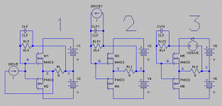
The circuit in the first post is suppose to have the advantage that only the output devices see the full supply voltage, and indeed this is true. The front end operates at +/-24V which could just as easily be half this amount for the same performance. The input stage only has to generate a signal equivalent to the gate-to-gate swing required to fully enhance the mosfets, which is about 14Vpp.
The output stage operates common-source, which in the advertising of the times was described as a "drain follower". At idle, the devices see the supply as +/-50V. As one device turns on and the other turns off, the supply is seen to swing from the extreme of +0,-100 and +100,-0 - not really to zero but you see the trend.
Feedback is taken from the floating supply centre-tap. The supply is built as any split-rail supply but not grounded directly. Instead, the mosfets pull the supply up and down and the speaker is driven from the supply CT. Feedback is taken from this point which puts a "crimp" in the power of the feedback loop. The feedback node is not directly regulated by the output devices, so performance of amplifiers like these is never as good as the conventional approach. The Trans Nova amps were essentially the same.
Some designers object to the fact that the power transformer interwinding capacitances have signal currents through them and signal voltages across them. This can cause outbound noise onto the mains in addition to introducing other supply modulations that can lead to instabilities of the amplifier. Clever designs tend to hold less promise than their novelty suggests.
The quality of the filter caps does not have to be any different than that for a conventional amp. of course, we are assuming long-life low-leakage caps are used, not voodoo "audio" caps nor low-grade junk.
Note: I'll admit to not having read the whole thread so the above should already have been covered...
Have fun
Last edited:
Feedback is taken from the floating supply centre-tap. The supply is built as any split-rail supply but not grounded directly. Instead, the mosfets pull the supply up and down and the speaker is driven from the supply CT. Feedback is taken from this point which puts a "crimp" in the power of the feedback loop. The feedback node is not directly regulated by the output devices, so performance of amplifiers like these is never as good as the conventional approach. The Trans Nova amps were essentially the same.
Some designers object to the fact that the power transformer interwinding capacitances have signal currents through them and signal voltages across them. This can cause outbound noise onto the mains in addition to introducing other supply modulations that can lead to instabilities of the amplifier. Clever designs tend to hold less promise than their novelty suggests.
The quality of the filter caps does not have to be any different than that for a conventional amp. of course, we are assuming long-life low-leakage caps are used, not voodoo "audio" caps nor low-grade junk.
Hi Struth,
I'd like to elaborate this point a bit more if you don't mind.
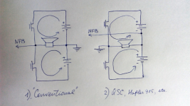
Let's look at the push-pull OPS from "fundamental" point of view. It fact, output devices control the way, the current from PSU flows through the load.
All the rest of the amplifier circuit provides the required voltage gain and the means of driving the output devices.
The closer PSU to ideal one (constant V, unlimited "I", zero impedance) - the better. No doubt.
Now - please see the picture. In fact, the only difference between (1) "conventional" OPS arrangement and (2) the one, utilised in QSC, Hafler 915 and some other amps, is the grounding point and the point where we take NFB from (opposite sides of the load).
What I'd like to say - your comments with regards to PSU issues (transformers, filtering caps) are true for both cases.
Some people also claim the 2-nd option never performs as good as the 1-st one. I disagree with that because of the considerations mentioned above. No principal difference.
What do you think?
Cheers,
Valery
Attachments
Last edited:
utilised in QSC, Hafler 915 and some other amps, is the grounding point and the point where we take NFB from (opposite sides of the load).
Worth to mention : https://linearaudio.net/article-detail/2224

Has anybody tried it ?
Hi Forr,
Good example

However, the word "audiophile" in the article looks like a certain exaggeration
Seems too "class B" to me.Here is the other one from Linear Audio with properly biased lateral FETs:
https://linearaudio.net/sites/linearaudio.net/files/May 28-Figure 9 - Full Amp.pdf
Cheers,
Valery
Has anybody tried it ?
I tried similar but much simpler solution, the link to pdf with scheme: http://www.diyaudio.com/forums/solid-state/57892-tcj-evolve-simply-good-amps-idea-2.html#post654105
I tried similar but much simpler solution, the link to pdf with scheme: http://www.diyaudio.com/forums/solid-state/57892-tcj-evolve-simply-good-amps-idea-2.html#post654105
Well, combination of these two - the one mentioned by Forr and Pawel's one - would form a very decent amplifier. I would also add a bias spreader - it's more or less ok to run as is at +/-15V rails, but at +/-25...50V, for example, thermal feedback is a must, if we are talking about IRFPs (laterals - a different story).
- Status
- This old topic is closed. If you want to reopen this topic, contact a moderator using the "Report Post" button.
- Home
- Amplifiers
- Solid State
- Could someone explain this Hafler/Strickland output topology to me?