Hi,
May someone explain me the point n°8 of the I2StoPCM Manual please, I can' understand the explanation !
Do have I to disassemble the LP5900sd if i feed the board with the 5V in/Gnd pins with a noiser external pre reg (4v to 6V) ?
What is the use of the Vin/Gnd/Vout pins on one side of the board? My understanding is it is just to regulate an external input and output this last with a clean 3.3 V ! But do I have to disassemble a reg chip on the board as well if not used ???? what is "the external lox noise regulator" ?
At least what is the use of the DC output/Gnd pins just near ? do theu output a clean 3.3 V also ?
thanks in advance
regards
Eldam
Hi Ian,
Does the TDA1541 need the I2StoPCM board to be in Half-speed mode please ? ("Job" + "half" jumpers selected !)
Source is the Wave I/O.
Thanks in advance if anybody else tried the I2StoPCM with the Wave I/O to feed the TDA1541A in simultanous mode.
It doesn't with the Amanero , if that is any help.
Yes, it heps a lot : same XOs speed !
Thank you very much.
Hummm have a very low voltage values on the TDA1541 pin 1 to 4
pin 1 0.25 V (LE/WS)
pin 3 & 4 (data R + L): 0.4 V !
pin 27 is - 5 V (simultaneous mode) : so OK.
the 3 orange leds on the I2StoPCM are ok ans is feed at 4.6 VDC ! Strap is on "JOB".
all uf-l signal path buzz through connector and cable also ! : so checked !
Do you use the output uf-l with Dr & Dl for data left and data right ?
Strannnnnnnnnnge !
Last edited:
Yes, it heps a lot : same XOs speed !
Thank you very much.
Hummm have a very low voltage values on the TDA1541 pin 1 to 4
pin 1 0.25 V (LE/WS)
pin 3 & 4 (data R + L): 0.4 V !
pin 27 is - 5 V (simultaneous mode) : so OK.
the 3 orange leds on the I2StoPCM are ok ans is feed at 4.6 VDC ! Strap is on "JOB".
all uf-l signal path buzz through connector and cable also ! : so checked !
Do you use the output uf-l with Dr & Dl for data left and data right ?
Strannnnnnnnnnge !
Can't remember, can post a pix in a day or so.
Hi Ian,
Does the TDA1541 need the I2StoPCM board to be in Half-speed mode please ? ("Job" + "half" jumpers selected !)
Source is the Wave I/O.
Thanks in advance if anybody else tried the I2StoPCM with the Wave I/O to feed the TDA1541A in simultanous mode.
Hi Eldam,
TDA1541 only needs PCM board running at half speed mode for 352/384KHz.
You don't need half speed mode for any lower Fs. But please conform the MCLK frequency is high enough. Please refer to PCM board user's manual.
Regards,
Ian
Hello Ian,
Thanks for your answer. So with the Wave I/O board which max XO is 24.xxx I should have a maximum of 192 K hz sampling rate !
TDA-1541 which can play at 384 Khz should be enough to play this rate with a 50 M XO...
Ok so no half mode speed with the Wave-IO.
It works fine since this afternoon ! (the low values was due to a problem on the - 15 V rail !
I shall test with two AD1862 then.
Thank you Ian and Supra
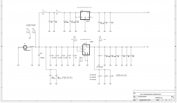
Schematic of Power supply section of PCM board
Here is the schematic of power supply section of I2S to PCM board.
Somebody wants to upgrade power supply by removing the on board LDO and replacing it with better external power supply. That's the reason I post the schematic here.
With fully understanding on the schematic, you will figure out how to hook up things together.
Basically there are two LDOs on board, one(U3) for CPLD and the other one(U4) for re-clocking. Both of them are 3.3V output. The second one can affect the sound quality, so is more important than the first one.
If you just want to remove U4, you have to keep 5V power connected to J6 to power CPLD (via U3), and hoop up external 3.3V power from TP5(3.3V VOUT) and TP6(GND) for re-clocking. For other options so on.....
Just hope there are some helps,
Ian
Attachments
Hi Ian,
Thank you for sharing these informations !
What sort of supply could be better instead U4 according to you ?
What can be improved ? Noise floor ? Anything else ?
Talking about u4, are there any embeded regs on the chain of the devices before which can be a limitation as well like reclocker : clockboard , Fifo (same regs as U4)???
Why just changing U4 could be enough in relation to the others regs of the devices before ?
PS : maybe a stupid question but what about the quality of the PS of the isolator chips (your board or any isolator chip) ? Just a simple stable voltage reg is enough for such a chip?
Last edited:
Hi Ian,
Thank you for sharing these informations !
What sort of supply could be better instead U4 according to you ?
What can be improved ? Noise floor ? Anything else ?
Talking about u4, are there any embeded regs on the chain of the devices before which can be a limitation as well like reclocker : clockboard , Fifo (same regs as U4)???
Why just changing U4 could be enough in relation to the others regs of the devices before ?
PS : maybe a stupid question but what about the quality of the PS of the isolator chips (your board or any isolator chip) ? Just a simple stable voltage reg is enough for such a chip?
Hi Eldam,
I always use batteries if I want to improve low noise power supply. Once system get improved, you can feel from focusing, 3D effect and the depth of the stage, mostly.
PCM board is based on synchronized logic design, so only MCLK and re-clocking section affects the finial signal quality, that's why U4 is more important.
There are many low noise power supply solutions,could be slightly different on result. You need give some try to find out your favorite. Shunt has better dynamic preference because of the Class A. But local bypassing also plays important part in high speed design.
Looking forward to your good news,
Ian
Thanks Ian,
Do you have a FR wide band and low enough impedance with your battery ? TSA7x reg are putted after with around 50 uF X7R ceramic smd caps ?
Or Avantage to the shunt because for a wide band FR range and low impedance against a less stable voltage output and noise in relation to the battery you use and very stable TSA7 regs ?
Is the stability of voltage about the pre reg a premium importance as far as it doesn't drop below the minimum needed for the low drop embeded smd regulators (and bove the maximum required voltage of course)?
To rephrase it : do a shunt stabiliser with 0.2 V drift could be good enough if the low drop smd regs are keeped as far as the noise floor is low enough ?
So :
First : noise floor
less important : impedance curve level and width of FR
Here is the schematic of power supply section of I2S to PCM board.
Somebody wants to upgrade power supply by removing the on board LDO and replacing it with better external power supply. That's the reason I post the schematic here.
With fully understanding on the schematic, you will figure out how to hook up things together.
Basically there are two LDOs on board, one(U3) for CPLD and the other one(U4) for re-clocking. Both of them are 3.3V output. The second one can affect the sound quality, so is more important than the first one.
If you just want to remove U4, you have to keep 5V power connected to J6 to power CPLD (via U3), and hoop up external 3.3V power from TP5(3.3V VOUT) and TP6(GND) for re-clocking. For other options so on.....
Just hope there are some helps,
Ian
Thank Ian,for Scheme and support
")
There are many low noise power supply solutions,could be slightly different on result. You need give some try to find out your favorite. Shunt has better dynamic preference because of the Class A. But local bypassing also plays important part in high speed design.
maybe this will fit the tight space?
Trident
Just as an experiment , I tried one of these cheap Ebay 1543 dacs with FIFO/isolator and double clock. No PCM-I2S as wont work with 1543. And it is only capable of 96Khz.
Surprisingly good, a bit raw perhaps but very musical and open, we compared it to a $10K+ new dac and it wasn't shamed at all. Obviously all of Ian's FIFO gear is doing what it is designed for.
But I have to turn dac off and manually reset clock (with reset button) every time I use it, anyone know what is going on?
Some of you were talking about different voltage regulators,
Has anyone tried the new LT3042 ??
LT3042 - 20V, 200mA, Ultralow Noise, Ultrahigh PSRR RF Linear Regulator - Linear Technology
Has anyone tried the new LT3042 ??
LT3042 - 20V, 200mA, Ultralow Noise, Ultrahigh PSRR RF Linear Regulator - Linear Technology
Hello,
I did read the first pages long time ago, than not the first 39, but could not find answer to :
What happens if I do not connect master clock ? For example because I do not have it from the raspberry pi board?
It wont work at all or it would get clock from the bit clock?
Thanks,
JG
I did read the first pages long time ago, than not the first 39, but could not find answer to :
What happens if I do not connect master clock ? For example because I do not have it from the raspberry pi board?
It wont work at all or it would get clock from the bit clock?
Thanks,
JG
- Home
- Source & Line
- Digital Line Level
- Drive NOS AD1865/62,PCM1704/02/63,TDA1541 from FIFO: Universal I2S-PCM driver board