The input stage is easy to understand, and is found in many (most?) "modern" (global feedback) transistor amps from the 60s and even some stuff from the early 70s. While eschewed now, it still offers some advantages.
The feedback is returned to the emitter of the input transistor. This is both AC and DC feedback. The emitter is biased by the DC output voltage. The DC gain is usually unity; the AC gain can be set with a resistor and DC blocking capacitor to signal ground.
One advantage of this configuration is that it presents one less pole to calculate for Nyquist stability, which brings us to your issue -
This is a likely scenario. Haphazard placement of poles will sometimes cause them to "stack up" and produce attenuation slopes of 12 dB/octave, which if inside the loop gain will likely cause oscillation or poor stability. This is why conventional designs often employ a "Miller capacitor" or Cdom or dominant capacitor. This method slows the circuit down so all slopes of more than 6 dB/octave occur well below unity gain.
When you mix and match active devices in an existing circuit, sometimes this strategy must be reworked. There are several approaches but in my opinion the best approach is to make the output stage as fast as possible and roll off the Vas stage so there's no gain in the trouble zone. 300 kHz is sufficient for audio.
The feedback is returned to the emitter of the input transistor. This is both AC and DC feedback. The emitter is biased by the DC output voltage. The DC gain is usually unity; the AC gain can be set with a resistor and DC blocking capacitor to signal ground.
One advantage of this configuration is that it presents one less pole to calculate for Nyquist stability, which brings us to your issue -
WRT the the devices, I expect the question is not so much what is the topology (circuit) but the actual devices used. This pertains to their ft or "speed" as compared with the original devices. Faster, newer devices may require a slightly different compensation scheme.
This is a likely scenario. Haphazard placement of poles will sometimes cause them to "stack up" and produce attenuation slopes of 12 dB/octave, which if inside the loop gain will likely cause oscillation or poor stability. This is why conventional designs often employ a "Miller capacitor" or Cdom or dominant capacitor. This method slows the circuit down so all slopes of more than 6 dB/octave occur well below unity gain.
When you mix and match active devices in an existing circuit, sometimes this strategy must be reworked. There are several approaches but in my opinion the best approach is to make the output stage as fast as possible and roll off the Vas stage so there's no gain in the trouble zone. 300 kHz is sufficient for audio.
The Mains Light Bulb is there for proving that you have wired it up correctly.
Then you power up directly and set the output bias.
You should not try to set the bias though the Mains Light Bulb Tester.
Have you tried testing into a open output?
or into 16r, or 8r0, or 4r0?
Then try 1nF//8r, then 3n3F//8r0,
do your testing it in stages.
600mW is also a small signal transistor, typically To92 package.
Medium power packages are typically To126, in 5W to 25W rating.
Last edited:
I usually wind up the variac slowly to monitor the device´s behaviour, with the bulb in series. I observed the oscillation starting with the 2µF capacitor and the bulb prevented bigger damage.
I thought I re-check the bias current, of course without the bulb, because I had soldered a wrong pot value in before, but then unfortunately on re-boot I forgot that the bulb was not there and damage was done.
Open works flawless, into a speaker as mentioned too, (with music programme),
into 8ohm load works flawless, 100nF/8R flawless. Others I have not tried.
4Ohm I think the amp is not designed for.
16Ohm and stepwise caps I try when I get the new output devices.
I scratch my head about the possibly bogus output devices. Reichelt is a renowned dealer, but surely no guarantee on the parts.
We had thousands of Tip142 darlingtons from them and all were flawless.
-helmut
The emitter is biased by the DC output voltage.
Geoff Moss has added a CCS to the singleton input stage like shown here: The Class-A Amplifier Site - A JLH Amp for the Quad ESL57. What does this contribute?
You say "The emitter is biased by the DC output voltage." - the output of the amp moves up and down with signal.
This stage is so different to any common emitter or common collector or whatever that I have difficulties to understand.
The 47pF compensation cap is located at the VAS stage, so it does roll of gain early.
-helmut
helmut, do you have a 'scope?
I forgot to ask.
You do need a scope.
Btw what is that blue thing flying over the rightmost output device?
What is the function of the red/black striped wire?
Do you have two channels? Or one?
Or dual mono amps, so each is identical? (even so I'd compare the two channels with the scope.)
With the scope and a resistive load, a look at a ~1kHz square wave will tell a bunch about what the amp is doing. If there is a parasitic it will likely show up with the square wave. You'll want to start with the input level nil and bring it up slowly while monitoring. Parasitics tend to "take off" as level increases.
If JLH published images of square wave response that would be useful for comparision.
Is the layout on your board JLH, or yours or someother??
_-_-bear
PS, did not spot a 47pf cap in the posted schematic?
PPS. mosfets sometimes like a larger gate ("stopper") resistor, and in some cases local HF degeneration on (iirc) the Nch side.
Folks,
to first answer the questions you implied, then those you asked.
I agree.
I bought Bob Cordell´s book and wanted to go through my design in analogy to the way he describes. Unfortunately I stumbled over the first stage, which I now know at least the name of. Reading an endless thread on matters that are 98% nothing to do with this subject did not promise anything. The class-A business is about an entirely different subject and has with the simple 30W amp just the first stage in common and the author.
Absolutely. Please appreciate that I never planned to have my problems with this amp solved by others, taking a shortcut. This was never my question. But now you offer specific help and I gladly accept.
Please appreciate that I just asked one question regarding the first stage. That is not related to any observations.
> What is your 'reactive load'?
As specified by JLH this is 8Ohm/2µF. The amp was stable BTW with 0.1µF
>What active devices are you using?
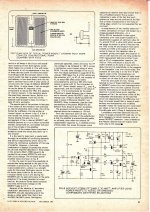
Compound transistor/ lateral mosfet pair, these days allegedly called "sziklai pair". Pls. see schematic for more.
>What is the frequency of the oscillation, and the amplitude?
Powering the amp up with a variac and a bulb current limiter I noticed HF fuzz riding on top of the sinewave. From memory, this was not as high frequent as I expected (MHz), rather below 100 kHz on a 1kHz wave.
>What quiescent are you using?
I adjusted the quiescent current to 100mA as recommended by JLH for lateral mosfets, but then forgot to plug the bulb limiter in again and on the next power-up the output devices blew. I now wait for new ones.
>What are your compensation values, and where?
Typical JLH compensation directly on the input device. JLH claimed total stabilty with 47pF and perfect square wave behavior.
>Can you show us a picture of both your schematic and your implementation?
attached. I used the 2S type transistors for the preamp stages and the 2N types for the output pair. In case you wonder about the funny transistor sockets. These are my "universal" footprints that let me accomodate any transistor during evaluation.
>And to add, measure all the base/emitter voltages on all active devices.
Currently not possible. Waiting for new output devices.
The amp ran for hours with an actual speaker, just failed the reactive test and thus is not unconditionally stable and reliable.
Reading in Bob´s Book I immediately detected a few possible layout shortcomings like insufficient local decoupling.
-helmut
donFolks,
to first answer the questions you implied, then those you asked.
I agree.
I bought Bob Cordell´s book and wanted to go through my design in analogy to the way he describes. Unfortunately I stumbled over the first stage, which I now know at least the name of. Reading an endless thread on matters that are 98% nothing to do with this subject did not promise anything. The class-A business is about an entirely different subject and has with the simple 30W amp just the first stage in common and the author.
Absolutely. Please appreciate that I never planned to have my problems with this amp solved by others, taking a shortcut. This was never my question. But now you offer specific help and I gladly accept.
Please appreciate that I just asked one question regarding the first stage. That is not related to any observations.
> What is your 'reactive load'?
As specified by JLH this is 8Ohm/2µF. The amp was stable BTW with 0.1µF
>What active devices are you using?
Compound transistor/ lateral mosfet pair, these days allegedly called "sziklai pair". Pls. see schematic for more.
>What is the frequency of the oscillation, and the amplitude?
Powering the amp up with a variac and a bulb current limiter I noticed HF fuzz riding on top of the sinewave. From memory, this was not as high frequent as I expected (MHz), rather below 100 kHz on a 1kHz wave.
>What quiescent are you using?
I adjusted the quiescent current to 100mA as recommended by JLH for lateral mosfets, but then forgot to plug the bulb limiter in again and on the next power-up the output devices blew. I now wait for new ones.
>What are your compensation values, and where?
Typical JLH compensation directly on the input device. JLH claimed total stabilty with 47pF and perfect square wave behavior.
>Can you show us a picture of both your schematic and your implementation?
attached. I used the 2S type transistors for the preamp stages and the 2N types for the output pair. In case you wonder about the funny transistor sockets. These are my "universal" footprints that let me accomodate any transistor during evaluation.
>And to add, measure all the base/emitter voltages on all active devices.
Currently not possible. Waiting for new output devices.
The amp ran for hours with an actual speaker, just failed the reactive test and thus is not unconditionally stable and reliable.
Reading in Bob´s Book I immediately detected a few possible layout shortcomings like insufficient local decoupling.
-helmut
According to Hood's original circuit the ground is close the output whereas the diagrams you have posted show this at the input.
The dirtiest earth returns need to go to ground first in order not to contaminate the negative feedback decoupling limb at the front end - as this requires a clean reference point. There is some resistance in wire and if the reference point is first in line to the resistance then it is going to be modulated by the output. You should research this and how star earth systems work .
The values of the stopper resistors in each limb of the output compound halves. The arrangements differ between the circuit diagrams you have posted. One shows each half having 330 ohms - the lower limb should be 1200 ohms. If that value is incorrect the loop gain will increase at HF whereas it is desirable that it decreases to less than one well before the feedback loop reaches 180 degrees of phase.
Last edited:
Geoff Moss has added a CCS to the singleton input stage like shown here: The Class-A Amplifier Site - A JLH Amp for the Quad ESL57. What does this contribute?
Linearity, gain, and voltage swing.
You say "The emitter is biased by the DC output voltage." - the output of the amp moves up and down with signal.
Of course. This network applies global feedback. It also provides DC stability. What's going on with no signal applied?
This stage is so different to any common emitter or common collector or whatever that I have difficulties to understand.
This topology has been applied extensively in early solid state amplifiers. There are many variations, but they all work basically the same.
It is an emitter feedback circuit. The voltage from emitter to Vee (ground in single ended circuits) tracks the voltage from the base to Vee. If the beta of the transistor is high enough, it can be ignored and the transfer function is for all practical purposes linear.
The 47pF compensation cap is located at the VAS stage, so it does roll of gain early.
Well you either need faster output devices, or a bigger Miller capacitor. You can try to figure out the Nyquist diagram
") D)or you can punt and try
D)or you can punt and try some bigger capacitors. If I were you, I'd punt and try some different capacitors.
Bear is giving you some very useful advice. If you don't have a scope and a seat of the pants understanding of transient response and damping, just try bigger Miller caps and see where it goes. Use the smallest value that provides the required stability.
I breadboarded the JLH amp out of salvage and spare parts when I was deciding on what kind of headphone amp to build. I thought it sounded awesome as a headphone amp. I didn't have the problems you're experiencing.
I will try to explain it to you in a simple and practical way. I hope I don't confuse you.
First, I credit Walt Jung for providing an explanation that I could understand and use. I highly recommend looking him up.
We must look at the phase shift inside the feedback loop. Phase shift can cause problems, including instability and oscillation. We will consider the case of an op amp with an output buffer and global feedback applied; a theoretical two stage global feedback circuit.
First case- Buffer has phase shift of 90 degrees at 1 MHz and op amp has phase shift of 90 degrees at 10 MHz. This will oscillate theoretically at 10 MHz because there will be plenty of loop gain at 10 MHz, and the phase shift will be 180 degrees. Actual frequency will be lower but we can see that this is a no-go. We also know that we will have to slow the op amp way down and we will realize that the buffer's 1 MHz bandwidth isn't much to work with. We must look at the datasheet's open loop gain vs frequency chart to juggle this.
Second case - Buffer has phase shift of 90 degrees at 1 MHz and op amp has phase shift of 90 degrees at 500 MHz. The buffer has virtually no gain (way less than 1) at 500 MHz, so theoretically the amplifier should be stable without compensation. This is a poor practice but it's been employed.
Third case - An actual design of mine. It's an LME49600 buffer + op amp of choice (I'm using a 5532 right now) with global feedback. Now the 49600 is way fast, with useable output up in the gigahertz range. (You can look it up if you want but it's super fast.) So in the case of a 5532 buffered with a 49600, there is no compensation required because the 5532 is doing nothing in the gigahertz range. In fact, I'm pretty sure that the 5532 has 180 degrees of phase shift way before 1 gigahertz. So this is for all practical purposes an ideal circuit; there will be no sorting of transients or instability because the circuit will behave exactly like the op amp used. In fact, the input impedance of the 49600 is in the megohm range so the op amp will always operate class A, driving virtually no load. This extracts the absolute maximum performance out of the op amp even when driving a load; it couldn't be closer to ideal for humble audio applications.
So in summary, you must look at the phase shift and you want a gain of less than 1 for phase shifts past around 135 degrees. If the gain is more than 1 at phase shift 180 degrees, you know what will happen.
I hope this helps you understand a little better.
First, I credit Walt Jung for providing an explanation that I could understand and use. I highly recommend looking him up.
We must look at the phase shift inside the feedback loop. Phase shift can cause problems, including instability and oscillation. We will consider the case of an op amp with an output buffer and global feedback applied; a theoretical two stage global feedback circuit.
First case- Buffer has phase shift of 90 degrees at 1 MHz and op amp has phase shift of 90 degrees at 10 MHz. This will oscillate theoretically at 10 MHz because there will be plenty of loop gain at 10 MHz, and the phase shift will be 180 degrees
. Actual frequency will be lower but we can see that this is a no-go. We also know that we will have to slow the op amp way down and we will realize that the buffer's 1 MHz bandwidth isn't much to work with. We must look at the datasheet's open loop gain vs frequency chart to juggle this.Second case - Buffer has phase shift of 90 degrees at 1 MHz and op amp has phase shift of 90 degrees at 500 MHz. The buffer has virtually no gain (way less than 1) at 500 MHz, so theoretically the amplifier should be stable without compensation. This is a poor practice but it's been employed.
Third case - An actual design of mine. It's an LME49600 buffer + op amp of choice (I'm using a 5532 right now) with global feedback. Now the 49600 is way fast, with useable output up in the gigahertz range. (You can look it up if you want but it's super fast.) So in the case of a 5532 buffered with a 49600, there is no compensation required because the 5532 is doing nothing in the gigahertz range. In fact, I'm pretty sure that the 5532 has 180 degrees of phase shift way before 1 gigahertz. So this is for all practical purposes an ideal circuit; there will be no sorting of transients or instability because the circuit will behave exactly like the op amp used. In fact, the input impedance of the 49600 is in the megohm range so the op amp will always operate class A, driving virtually no load. This extracts the absolute maximum performance out of the op amp even when driving a load; it couldn't be closer to ideal for humble audio applications.
So in summary, you must look at the phase shift and you want a gain of less than 1 for phase shifts past around 135 degrees. If the gain is more than 1 at phase shift 180 degrees, you know what will happen.
I hope this helps you understand a little better.
Last edited:
Linearity, gain, and voltage swing.
Well you either need faster output devices, or a bigger Miller capacitor. You can try to figure out the Nyquist diagram
some bigger capacitors. If I were you, I'd punt and try some different capacitors.
Bear is giving you some very useful advice. If you don't have a scope and a seat of the pants understanding of transient response and damping, just try bigger Miller caps and see where it goes. Use the smallest value that provides the required stability. Oscillation might not be detected with an elementary scope.
The 47 p.f. capacitor does not perform a Miller function. It bypasses the output stage ensuring the input and Vas transistor pairing is stable regardless of any misbehavior of the output combinations. The problem with MOSFET's is that they can be too fast for their own good - and you might not witness this on some oscilliscopes.
Last edited:
Phew. Many Questions.
Yes I have a scope. 60Mhz.
>Btw what is that blue thing flying over the rightmost output device?
This is a remnant of the last thing I tried. It is a 100pF mica cap over the emitter resistors in the output stage - lead compensation JLH recommended if necessary on the darlington version. Did not work.
>What is the function of the red/black striped wire?
This is a more solid earth connection to the local bypass cap than the PCB tracks provide. I suspected that those are badly layed out. The first thing that needs rework if I make a re-design of the PCB.
>Do you have two channels? Or one?
No this is a mono amp for instrumental use.
>If JLH published images of square wave response that would be useful for comparision.
I will upload the whole thing as soon as I have a chance.
>Is the layout on your board JLH, or yours or someother??
Mine. JLH´s layout is part of the upload then. If you see how unspectacular it looks
you wonder if had put any special effort into HF layout.
> PS, did not spot a 47pf cap in the posted schematic?
From the input stage to the VAS.
>According to Hood's original circuit the ground is close the output whereas the >diagrams you have posted show this at the input.
That is true. I noticed the wrong path and made a more direct connection direct at the output devices, which you see on the photos.
The high current tracks are thus away from the quiet ones.
>PPS. mosfets sometimes like a larger gate ("stopper") resistor, and in some cases local HF degeneration on (iirc) the Nch side.
I tried 330Ohm gate stoppers - no change. JLH did not mention them in three updates. I thought the Sziklai pair was better in this respect.
>The values of the stopper resistors in each limb of the output compound halves differ
In the original article he uses different ones. In a later article (the one uploaded for better readability) he uses equal ones again. Sometimes there is a lot of guesswork why JLH did things.
I have to go out of house and attend later again.
-helmut
Hi Helmut,
You have a lot of very good advice here from some clever person, Ian, Don, etc......
Thanks for the schematic. Singleton current global fb, ring of two CCS supplying a npn VAS (Q3?), single bias generator (R15/C5), hybrid bipolar/lateral fet CFP output stage, Zobel and interesting R4 series outside the fb. Single phase lead capacitor C4/47pF for stability. Quite a few variations of the original JLH 1969, which astonished me for its performance in fact 1969. Damn, I'm that old........
A few observations. Given that this is a current fb amp, the values of R10/22k and R15/820R are a bit high. To reduce the voltage drop across R10 (which I would assume around 2.5V, a little high) and to increase the stability of the VAS I would decrease R11 from 4k7 to 1K, increasing collector current through the VAS from a miserly 150uA up to 660uA or so and then reduce R10 (22k) down to 2k2 and R15 (820R) down to 82R. This will give more drive to the VAS output, which will cope better with the bias variations of the output stage at crossover variations, specifically addressing the very low transconductance of the output devices (around 0.7S).
To accommondate these changes, I'd change C5 to 470uF, C7 to 220uF, and add some Miller capacitance of 22pF across collector to base of VAS Q3, the BC447. Then reduce C4 phase lead, to around 15pF.
You would finally need to change R15 to 220R.
These are not verified with simulation; merely my experience and likely a bit off. However, I'm not that happy about the very high fb resistors; the noise and drive issues do improve by reducing them and in fact the dependent on the CCS is a weakness (on my amps I take ALL singleton current from the output node, rather than adding extra current from a CCS as I find this reduces noise).
BTW, I would say that if the amp is stable with 8R//0.1uF rather than 2uF it is pretty good, since the more relevant test is 0.1uF if you are not using an ESL63. These tests are very tough for AB amps, and noting that you are using just 100mA quiescent, low transconductance and very tetchy bipolar drivers the crossover transition is, well, difficult.
This is an interesting circuit, and I know it sounds very, very good, but when you move to different, modern devices you come up across a new Nyquist regime to bring to heel the much faster modern transistors.
I hope this, and other advice, is helpful.
Cheers,
Hugh
You have a lot of very good advice here from some clever person, Ian, Don, etc......
> What is your 'reactive load'?
As specified by JLH this is 8Ohm/2µF. The amp was stable BTW with 0.1µF
>What active devices are you using?
Compound transistor/ lateral mosfet pair, these days allegedly called "sziklai pair". Pls. see schematic for more.
>What is the frequency of the oscillation, and the amplitude?
Powering the amp up with a variac and a bulb current limiter I noticed HF fuzz riding on top of the sinewave. From memory, this was not as high frequent as I expected (MHz), rather below 100 kHz on a 1kHz wave.
>What quiescent are you using?
I adjusted the quiescent current to 100mA as recommended by JLH for lateral mosfets, but then forgot to plug the bulb limiter in again and on the next power-up the output devices blew. I now wait for new ones.
>What are your compensation values, and where?
Typical JLH compensation directly on the input device. JLH claimed total stabilty with 47pF and perfect square wave behavior.
>Can you show us a picture of both your schematic and your implementation?
attached. I used the 2S type transistors for the preamp stages and the 2N types for the output pair. In case you wonder about the funny transistor sockets. These are my "universal" footprints that let me accomodate any transistor during evaluation.
>And to add, measure all the base/emitter voltages on all active devices.
Currently not possible. Waiting for new output devices.
The amp ran for hours with an actual speaker, just failed the reactive test and thus is not unconditionally stable and reliable.
Thanks for the schematic. Singleton current global fb, ring of two CCS supplying a npn VAS (Q3?), single bias generator (R15/C5), hybrid bipolar/lateral fet CFP output stage, Zobel and interesting R4 series outside the fb. Single phase lead capacitor C4/47pF for stability. Quite a few variations of the original JLH 1969, which astonished me for its performance in fact 1969. Damn, I'm that old........
A few observations. Given that this is a current fb amp, the values of R10/22k and R15/820R are a bit high. To reduce the voltage drop across R10 (which I would assume around 2.5V, a little high) and to increase the stability of the VAS I would decrease R11 from 4k7 to 1K, increasing collector current through the VAS from a miserly 150uA up to 660uA or so and then reduce R10 (22k) down to 2k2 and R15 (820R) down to 82R. This will give more drive to the VAS output, which will cope better with the bias variations of the output stage at crossover variations, specifically addressing the very low transconductance of the output devices (around 0.7S).
To accommondate these changes, I'd change C5 to 470uF, C7 to 220uF, and add some Miller capacitance of 22pF across collector to base of VAS Q3, the BC447. Then reduce C4 phase lead, to around 15pF.
You would finally need to change R15 to 220R.
These are not verified with simulation; merely my experience and likely a bit off. However, I'm not that happy about the very high fb resistors; the noise and drive issues do improve by reducing them and in fact the dependent on the CCS is a weakness (on my amps I take ALL singleton current from the output node, rather than adding extra current from a CCS as I find this reduces noise).
BTW, I would say that if the amp is stable with 8R//0.1uF rather than 2uF it is pretty good, since the more relevant test is 0.1uF if you are not using an ESL63. These tests are very tough for AB amps, and noting that you are using just 100mA quiescent, low transconductance and very tetchy bipolar drivers the crossover transition is, well, difficult.
This is an interesting circuit, and I know it sounds very, very good, but when you move to different, modern devices you come up across a new Nyquist regime to bring to heel the much faster modern transistors.
I hope this, and other advice, is helpful.
Cheers,
Hugh
I stated 4r0......................
4Ohm I think the amp is not designed for................
NOT 4ohm.
An 8ohms capable amplifier should always be able to drive a 4r0 test load. Although at full power this will result in excessive dissipation and the test MUST be curtailed BEFORE the amp gets too hot.
I now test to 1/3rd of rated impedance to prove that the CURRENT capability of the amplifier is up to spec.
i.e. you can test an 8ohms capable amplifier with 2r7, for the two or three seconds it takes to see the DMM voltage settle to final value. Let it cool and repeat. A switch that increases input voltage by a factor of exactly 10times is good for this. The scope pic and the voltmeter read the 1/10th values and you change both to be ready to read the full values. Flick the switch and you get your readings, in general at about one second and flick back to low level.
Last edited:
Thanks for your help everybody.
Sorry, I fail to understand what you are driving at. A precision 4.0 Ohm dummy resistor?
The test procedure you suggest I suppose comes as soon as the amp is stable otherwise.
I explained that one with what I have read with D. Self: it is what many contemporary mosfets have on the output: a coil wound over a resistor. The coil gets active at HF. Self states that the resistor alone is better, because the coil might induce ringing, but it drops some power.
Self also questions the 2µF method. He thinks a .1 µ load is much harder for an amp. That´s where I have the value from and why I tried it.
I stick my nose into the suggestions y´all made and attend tomorrow. The scans are coming.
cheers,
-helmut
I stated 4r0.
NOT 4ohm.
Sorry, I fail to understand what you are driving at. A precision 4.0 Ohm dummy resistor?
The test procedure you suggest I suppose comes as soon as the amp is stable otherwise.
AKSA said:interesting R4 series outside the fb
I explained that one with what I have read with D. Self: it is what many contemporary mosfets have on the output: a coil wound over a resistor. The coil gets active at HF. Self states that the resistor alone is better, because the coil might induce ringing, but it drops some power.
Self also questions the 2µF method. He thinks a .1 µ load is much harder for an amp. That´s where I have the value from and why I tried it.
I stick my nose into the suggestions y´all made and attend tomorrow. The scans are coming.
cheers,
-helmut
The 47 p.f. capacitor does not perform a Miller function. It bypasses the output stage ensuring the input and Vas transistor pairing is stable regardless of any misbehavior of the output combinations. The problem with MOSFET's is that they can be too fast for their own good - and you might not witness this on some oscilliscopes.
Yes, you're correct. I'm in the habit of calling dominant poles imposed by capacitors "Miller capacitors." But in fact, the Miller effect is a very specific phenomenon. Application of these schemes (including using a Miller capacitor) are means to the same end, although they all work a little differently.
My prototype did not use Mosfets; it used MJE3055's. One small capacitor was employed to tame it, although it appeared stable without it.
The MOSFET version of Linsley-Hood's originated from a version where the output compound consisted of small signal transistors and Power Darlington transistors, so the use of MJE3055 and complement is a different animal.
I think your problem is likely to arise because of oscillation around the output compound pairs as this can be induced by the circuit layout and wiring and roaming free around these. Linsley-Hood claimed his MOSFET amplifier was stable without any compensation capacitors and your circuit ought not to behaving abnormally.
From what I can make from your photo's the power supply is integral with the amplifier on the same board and you need to be able to operate the amplifier without having it blow up.
One method of setting up amplifiers is to fit wire wound resistors between the power supply and the amplifier proper. The current draw can then be worked out from Ohms law by measuring the voltage drop across the wire wound resistor for one channel at a time.
As a starting point 100 ohm and 10 or more watts. A moistened finger on the body of the resistor and the other on the power switch will give you a gauge on the problem and allow quick reactions to prevail if there is a serious problem. If this test is passed you can try measuring some circuit voltages and adjusting the standing current if that is possible. You could also see if there is any change if you touch or move any leads connected to the printed circuit board. You could try that approach in case to rule out the possibility of cold solder joints. If you can get one channel working correctly you can make cross comparisons if the other is not so.
As an aside Linsley-Hood deplored the use of "Miller" capacitors to determine the dominant pole - you won't find them in any of his designs which used the simple single transistor form of Vas such as this. There are more elaborate ways to use "Miller" capacitors analogous perhaps to using two people where the job requires.
If used here a "Miller" capacitor from collector to base, the collector would be fed by the constant current source. At the base end the current feed comes from the collector load resistor of the Class A input transistor.
In that way the available ac charging currents in either direction are fixed by the respective dc operating conditions of the circuit elements at either end of the "Miller" capacitor.
Also the Vas is an inverting amplifier with HF fed back from collector to base in negative phase. This rolls off HF response with increasing frequency - requiring more current to be fed into the base to maintain the same level.
This has implications of a disabling effect if a rapid step up in level is required by the input signal and the dc current conditions cannot meet the instantaneous ac need.
Last edited:
The MOSFET version of Linsley-Hood's originated from a version where the output compound consisted of small signal transistors and Power Darlington transistors, so the use of MJE3055 and complement is a different animal.
I think your problem is likely to arise because of oscillation around the output compound pairs as this can be induced by the circuit layout and wiring and roaming free around these. Linsley-Hood claimed his MOSFET amplifier was stable without any compensation capacitors and your circuit ought not to behaving abnormally.
From what I can make from your photo's the power supply is integral with the amplifier on the same board and you need to be able to operate the amplifier without having it blow up.
One method of setting up amplifiers is to fit wire wound resistors between the power supply and the amplifier proper. The current draw can then be worked out from Ohms law by measuring the voltage drop across the wire wound resistor for one channel at a time.
As a starting point 100 ohm and 10 or more watts. A moistened finger on the body of the resistor and the other on the power switch will give you a gauge on the problem and allow quick reactions to prevail if there is a serious problem. If this test is passed you can try measuring some circuit voltages and adjusting the standing current if that is possible. You could also see if there is any change if you touch or move any leads connected to the printed circuit board. You could try that approach in case to rule out the possibility of cold solder joints. If you can get one channel working correctly you can make cross comparisons if the other is not so.
As an aside Linsley-Hood deplored the use of "Miller" capacitors to determine the dominant pole - you won't find them in any of his designs which used the simple single transistor form of Vas such as this. There are more elaborate ways to use "Miller" capacitors analogous perhaps to using two people where the job requires.
If used here a "Miller" capacitor from collector to base, the collector would be fed by the constant current source. At the base end the current feed comes from the collector load resistor of the Class A input transistor.
In that way the available ac charging currents in either direction are fixed by the respective dc operating conditions of the circuit elements at either end of the "Miller" capacitor.
Also the Vas is an inverting amplifier with HF fed back from collector to base in negative phase. This rolls off HF response with increasing frequency - requiring more current to be fed into the base to maintain the same level.
This has implications of a disabling effect if a rapid step up in level is required by the input signal and the dc current conditions cannot meet the instantaneous ac need.
Sorry Eddie about my incorrect attribution to ownership of the MOSFET problem to your project.
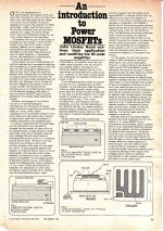
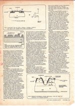
I have scanned the original article authored by Linsley-Hood which is self explanatory.
Thank you! I wish I'd seen that back when, a few years later, I was struggling with many of the issues he mentions.
Frankly, so were a number of the professors (many, many power mosfets died unnecessarily
)But academia prefers peer reviewed articles in "respected" journals - at least those journals provided references to other work (unlike many trade magazines)
- Status
- This old topic is closed. If you want to reopen this topic, contact a moderator using the "Report Post" button.
- Home
- Amplifiers
- Solid State
- JLH 1969 first amplification stage, need explanation