The input buffer is cascoded by the second pair of transistors which hold their Vce constant. Yes, it can be a Baxandall, cascode and buffer all in one. These names are all ideas, and they are not mutually exclusive.
You can check for yourself in the simulator. See the attached plot. Yes, the base current of one transistor is positive and the base current of the other transistor is negative. But they respond in phase to the AC input signal. When the input voltage rises, both bases draw more current. While the idle currents cancel because they are opposite phase (+ and -) the AC currents do not because they are in phase.
There is some kind of input current distortion cancelation.
Attachments
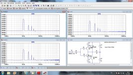
Okay, that is a cancellation of the 2nd harmonic, not a cancellation of the total current. Notice that the fundamental behaves additively as I showed.
What happens if you use a few different BC5xx model? Does the H2 cancellation change much with transistor properties or stay basically the same?
There are 3 "input stage currents":
1: DC quiescent currents.
2: AC input currents.
3: Error currents as proportion of the AC input currents.
These all behave differently, and each case needs to be treated uniquely.
Last edited:
Using source resistor for MOSFET
Hi Mr Cordell
I am reading page 233 of your book about source resistor to reduce the gm droop. You gave only one example of 0.15 ohm for IRFP240 and 0.22 ohm for IRFP9240. Is there any general formula to choose the source resistance for different MOSFET like BJT that you choose a value to drop 26mV with bias current?
Thanks
Hi Alan,
This is a good question. As far as I know, there is no formula for biasing the MOSFET output stage to an optimum as there is for the BJT. With the BJT there is a reasonably clear theoretical optimum (the 26mV number) that balances under-bias (gm droop) against over-bias (gm doubling). With MOSFETs, it is nearly impossible to get them to the point where there is too much gm at crossover. In any case, that level of bias is usually impractically high. I tried it with an IRFP240/9240 pair and even at 450mA bias the gm at idle just barely got up to the gm at large output currents of either polarity. BTW, this design probably would have sounded quite good because of the large class A region up to peak currents of nearly 1A and due to smaller thermal swings in the output stage with program material since it was running fairly hot even at idle (what I have dubbed a somewhat isothermal class AB design).
Bottom line is that in most practical cases for idle bias setting of MOSFET output stages, more is better (within thermal constraints). With regard to using source resistors and possible asymmetry of them, I think the choice is largely governed by ad-hoc experimentation in simulation to get the best-looking wingspread while using the best available MOSFET models. This is not to say that such experimentation can/should not be done on a working prototype while looking for the best THD compromise.
Cheers,
Bob
Very good one.... have beated mine Dx Mark One.
Well....it can go lower if i figure out how to use 33pf as compensation
Your amplifier goes much lower than 0.0048% loaded with 8 ohms.... but have to tweak and get out from the exactly calculated values..some drift from the optimize values reduces THD.... some out of the box thinking.
Your Cascode VAS is a great contribution to our community.... great one.... i may use your circuit if i figure out (or if you help me) how to use 33pf as compensation.
regards,
Carlos
When using a triple darlington output stage like the figure from Cordells book, use a small value of shunt compensation in addition to the miller compensation. The value can be kept quite small and it wouldnt necessarily increase the distortion but it will take care of the stability problems when using triples. For that amp try from 10 pf to 47 pf from vas collector to GND.
Hi Alan,
Bottom line is that in most practical cases for idle bias setting of MOSFET output stages, more is better (within thermal constraints). With regard to using source resistors and possible asymmetry of them, I think the choice is largely governed by ad-hoc experimentation in simulation to get the best-looking wingspread while using the best available MOSFET models. This is not to say that such experimentation can/should not be done on a working prototype while looking for the best THD compromise.
Cheers,
Bob
Hi Bob,
Does this hold true for your HEC output stage? In my sims, have found that around 150mA or a little lower gives better THD than higher biases.
Not sure about reality as I only have basic test equipment.
Many thanks,
Paul
Hi Mr Cordell
Thanks for your answer. IRFP240 and 9240 are readily available. So if I use 0.15 ohm for IRFP240 and 0.22 ohm for IRFP9240, and run at higher current than 150mA, I should get less crossover distortion?
I am planning to design with +/-40V rail voltage. If I run a 300mA bias current, power dissipation per transistor is 40V X 0.3A=12W. So if I use 3 pairs of power transistor, then the total dissipation is 12W X 6=72W/channel or 144W of heat generated for the stereo amp?
Assume I swing +/-30V, and load is 4ohm, then peak current is 30V/4ohm=7.5A and the RMS power output is (0.707 X 30V) X (0.707 X 7.5A) = 112W RMS output. With 0.3A bias per stage, total bias of 3 stages is 0.9A. The amp will be working in Class A in the first 1.8A output current. So the peak voltage operating in Class A is 1.8A X 4ohm = 7.2Vpeak. So the output power in total Class A is 0.5 X (7.2)2 /4ohm = 6.48W.
That sound very reasonable. 144W of heat, 112W Class AB power with 6.5W pure Class A power.
Does this sound reasonable to you?
Thanks
This is a good question. As far as I know, there is no formula for biasing the MOSFET output stage to an optimum as there is for the BJT. With the BJT there is a reasonably clear theoretical optimum (the 26mV number) that balances under-bias (gm droop) against over-bias (gm doubling).
Unless of course you drop half a volt on the ballast resistor.

When using a triple darlington output stage like the figure from Cordells book, use a small value of shunt compensation in addition to the miller compensation. The value can be kept quite small and it wouldnt necessarily increase the distortion but it will take care of the stability problems when using triples. For that amp try from 10 pf to 47 pf from vas collector to GND.
Good point,
I have found this to be helpful in some cases as well. I have often used a Zobel-like R-C combination with R in the range of 100 ohms. Output Triples like to be driven by a resistive-looking source of reasonably low impedance at high frequencies. The low output impedance at high frequencies naturally provided by the shunt feedback of Miller compensation is often sufficient, but not always, since any feedback-created output impedance will usually ultimately rise with frequency and look somewhat inductive. The C shunt or R-C shunt tends to take over from the VAS output impedance at higher frequencies, mitigating this concern.
Cheers,
Bob
When using a triple darlington output stage like the figure from Cordells book, use a small value of shunt compensation in addition to the miller compensation. The value can be kept quite small and it wouldnt necessarily increase the distortion but it will take care of the stability problems when using triples. For that amp try from 10 pf to 47 pf from vas collector to GND.
What is shunt compensation? I don't understand the term.
What is shunt compensation? I don't understand the term.
Hi Alan,
In this context, shunt compensation is the connection of a shunting network from the signal node, here the output of the VAS, to ground. Such a network tends to reduce gain of the VAS at high frequencies because the impedance of the shunt network goes down with frequency. The network is often a simple capacitor or a resistor in series.
This is in contrast to Miller compensation, which a feedback-based form of compensation that reduces gain at high frequencies.
Amplifiers can be compensated solely with shunt compensation or solely with Miller compensation. Miller compensation is more popular because it doesn't just throw the gain away to make it go down, but rather uses that gain as local feedback around the VAS, further linearising the VAS.
In the case being discussed, the primary compensation for the amplifier is Miller compensation, but some shunt compensation is added to help out a bit just at higher frequencies.
Cheers,
Bob
Bob, the formula for the optimal BJT bias point is based on the exponential Re slope of 27mV/octave. Since MOSFETs are typically biased close to subthreshold conduction which would be 75mV per octave or so, a similar rule would apply. However the transition to square-law behavior makes this more complicated. I think the optimal bias point will be at both an optimal Id and specific source resistance. And unlike for BJTs, this point will probably change with temperature. And of course it will be different between vertical and lateral types.
Last edited:
And unlike for BJTs, this point will probably change with temperature.
KT/q?Bob, the formula for the optimal BJT bias point is based on the exponential Re slope of 27mV/octave. Since MOSFETs are typically biased close to subthreshold conduction which would be 75mV per octave or so, a similar rule would apply. However the transition to square-law behavior makes this more complicated. I think the optimal bias point will be at both an optimal Id and specific source resistance. And unlike for BJTs, this point will probably change with temperature. And of course it will be different between vertical and lateral types.
Ideally, one would like to think this. However, just run a few wingspreads with MOSFETs and you will see that it is nearly impossible to get the transconductance of the output stage (the sum of the operating transconductances of the P and N devices) to become equal to that of either device when delivering high current. I termed this "transconductance droop" when I wrote up my MOSFET power amplifier back in 1983.
The practical starting point is to take a pair of verticals, like IRFP240 and 9240, and bias them at 150mA, a reasonable value. Do this with no source resistors. Look at the output stage transconductance, or gain into 8 ohms, at zero output current (e.g., 0V out). Then look at the transconductance at a significant output current, perhaps 5A. You will see that the transconductance at 0A output (crossover) is quite a bit smaller than at 5A output. This is transconductance droop.
Now increase that idle bias current to larger and larger values. You will see less and less gm droop at crossover, but almost never get to the point where there is no droop. You will get close if you bias these MOSFETs at about 0.5A, but for most this is considered an impractically high value.
Now, if you want to, introduce source resistors of whatever value you want. You will probably find that with adequate source resistance introduced you will be able to achieve low or no transconductance droop. Now you will think you have found an optimum value, perhaps akin to the 26mV rule. Unfortunately, you will find that the value of source resistance you had to add was a value so high as to be completely bad, killing the gm of the output stage and its ability to source large current into the load without wasting voltage headroom and power dissipation in the source resistors.
Cheers,
Bob
If my math is right, thermal voltage for BJTs (25.85mV at 300K) increases by about 86.2nV per C. So if your BJTs go up to 125C, the optimal bias point will now be near 34.5mV. So it increases by 1/3 at full power. In Lfets you have the same thing, but worse because the square-law region has its own tempco and the two laws of curves are interacting.
But that is assuming the optimal point is anywhere near subthreshold conduction.
EDIT: So there is not really a "null point" for MOSFETs, just diminishing returns. Hmm. Unless you use them only in class A at low currents within the subthreshold region where they can be treated somewhat like BJTs, but that would not make a power amp.
Last edited:
When using a triple darlington output stage like the figure from Cordells book, use a small value of shunt compensation in addition to the miller compensation. The value can be kept quite small and it wouldnt necessarily increase the distortion but it will take care of the stability problems when using triples. For that amp try from 10 pf to 47 pf from vas collector to GND.
Such a cap has little to nothing to do with stabilizing the triple, but with compensating the Miller loop which, in particular if a beta enhancer is used, may have stability issues. If you disagree, I would be happy to listen to any proof you may have. I am in particular curious how do you analyze the triple stability and estimate the stability margins
.Even so, simply a shunt cap is an unnecessary brutal Miller loop compensation method; a lead lag network (that is, a RC series) will save precious loop gain, while providing a very similar stability margin.
MOSFETs are typically biased close to subthreshold conduction which would be 75mV per octave or so
60mV/decade (theoretically), in practice it may be a tad higher.
The low output impedance at high frequencies naturally provided by the shunt feedback of Miller compensation is often sufficient, but not always, since any feedback-created output impedance will usually ultimately rise with frequency and look somewhat inductive. The C shunt or R-C shunt tends to take over from the VAS output impedance at higher frequencies, mitigating this concern.
A low source impedance is ideal for any EF, double or triple, anybody can see in simulation how the distortions are increasing with increasing the source impedance.
I don't think the source impedance has any major role in the triple EF stability. In fact, IIRC, the EF triple stability is improving with the source impedance, zero source impedance is kind of worst case.
- Home
- Amplifiers
- Solid State
- Bob Cordell's Power amplifier book