The present "simple TL431 circuit" uses seven components. I wonder whether a lavish increase to eleven components, would give roughly similar performance while eliminating low-voltage concerns and cant-find-a-SPICE-model-I-trust concerns.
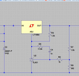
If this were my problem, and thank god it is not, I might consider something along the lines of the attached sketch, as a first possibility. The designer has the freedom to select among different amplifiers with different Gain-Bandwidth Products; one is not stuck with whatever GBW the mfr happened to put in their TL431 clone. If a Linear Technology amplifier is chosen, this increases the likelihood that the datasheet will include the openloop gain and phase; AND it increases the likelihood that the vendor-supplied SPICE model will match the datasheet quite well.
An external amplifier with external feedback resistors allows gain to be traded off against bandwidth by simply adjusting a single resistor (R3). You can dial up any phase margin you like. If the opamp GBW is much much greater than the IC voltage regulator's GBW, the opamp contributes very little "excess phase" to the cascade-of-amplifiers, and so it has only a small effect upon stability margins. LT sells some nice little opamps that work from 2V to 12V and have GBW in the neighborhood of 10 MHz. (So do other makers, of course; but now you're back in the should-I-trust-this-SPICE-model conundrum.)
Most of the extra components are squandered on the purifier circuit at far left. Node "A" is a DC voltage comfortably above the opamp's minimum supply requirement, and also comfortably below the regulator's output voltage. For a 12V regulator I'd set VA= 8volts, and for a 3.3V regulator I'd set VA= 2.7volts. At startup, the opamp's power supply pin is fed from node "A"; once the regulator wakes up and starts regulating, the second diode begins to conduct and the error amplifier is powered from the regulator output.
Attachments
cant-find-a-SPICE-model-I-trust concerns.
Indeed this was becoming a real concern of mine after I took a close look at the small signal gain versus frequency charts in the datasheets of each of the TI TL431 and the Exar SPX431LAN and XRP431L given how delicately such a circuit needs to be stabilised. (Perhaps you saw my inquiry on the LTspice Yahoo forum...)
Thanks - I will take a closer look at the circuit in your sketch.
PS: without wanting to take a massive detour, I was intrigued at the nature of these regulator circuits
Those fidelityaudio.co.uk guys might be onto something: replacing the high-fT bipolar output transistor, with an even-higher-fT MOS Field Effect Transistor. The NXP MOSFETs whose models come with LTSPICE are super-duper, but we can't buy those in the States. Even the runner up company (IR) makes MOSFETs that improve voltage regulator bandwidth: (Here's a link) and I copied the plot below. Just by changing the series pass element from BJT (green plot) to MOSFET (red plot), and leaving everything else unchanged, the regulator's bandwidth increased.
Attachments
I might consider something along the lines of the attached sketch, as a first possibility.
So...
- use something like an LM329 or LM4040-2.5 to set Vref for the op amp (I need to check fit for either to fit the same board)
- set R4 to provide enough current for the zener to operate properly
- Vout = Vref x (R1+R2)/R2 (as before)
For some reason the modelling I have done thus far - just basic operation of a 12V circuit - is very sensitive to load. Anything above 2A (with 19V Vsource) and it all goes splat. Presumably because a component is failing. In contrast, 5A was possible with 19V input in the former circuit. I will keep checking my work.
Isn't this just a step or two from a discrete version of a TL431/SPX431 etc? I wonder what the advantages/disadvantages might be of going further. I was also trying to relate this construction to the Jung/Didden super-regulator and the Fidelity Audio description of their regulator (I own one in 12V - at times it would seem awfully efficient to buy a 5V and 3.3V and move on but that wouldn't teach me much). Here the op amp is 'driving' the adjust pin of the LT1084 whereas in those circuits the op amp drives a pass BJT or power MosFET. It would be good to understand these better.
After a good deal of reading I think I now have a better grasp of series pass transistor regulators, although I am a long way from understanding the intricacies of the Jung/Didden super regulator.
How does one determine the GBW of the LT1084? I ask because if I model with the low noise LT1677 op amp (GBW 7.2MHz) which we used in our earlier measurement circuit discussions in lieu of the LT1797 (10MHz) things oscillate at gain settings which are fine for the LT1797.
(I still haven't gotten to the bottom of the load constraints issue but will try to find some time to look at it further today.)
If the opamp GBW is much much greater than the IC voltage regulator's GBW, the opamp contributes very little "excess phase" to the cascade-of-amplifiers, and so it has only a small effect upon stability margins.
How does one determine the GBW of the LT1084? I ask because if I model with the low noise LT1677 op amp (GBW 7.2MHz) which we used in our earlier measurement circuit discussions in lieu of the LT1797 (10MHz) things oscillate at gain settings which are fine for the LT1797.
(I still haven't gotten to the bottom of the load constraints issue but will try to find some time to look at it further today.)
(Here's a link) and I copied the plot below. Just by changing the series pass element from BJT (green plot) to MOSFET (red plot), and leaving everything else unchanged, the regulator's bandwidth increased.
How are you generating these (bode?) plots?
When I have been looking at stability I have been breaking the feedback loop, injecting a small signal AC voltage source and measuring -Vout/Vx where Vx is voltage on the other side of the injected AC voltage source; this I understand to be Loop Gain. I then look at phase margin Loop Gain is unity (zero dB). I ask because at no point are the plots flat like the ones you (and Jack) presented.
Attachments
Mark Johnson said:Those fidelityaudio.co.uk guys might be onto something: replacing the high-fT bipolar output transistor, with an even-higher-fT MOS Field Effect Transistor. The NXP MOSFETs whose models come with LTSPICE are super-duper, but we can't buy those in the States.
Mark, what about ZXMN7A11, SOT-223 or DPAK, available from Mouser? Spice model HERE
Sorry for OT.
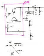
A common mistake people often make, is to forget that the loop breaker must close the feedback loop at DC*, while at the same time opening the feedback loop at all conceivable input signal frequencies. I personally like to have oodles of safety margin, so for audio work I choose to position the loop breaker pole at or below 1/(100 x OpenLoopGain) Hertz. Don't ask me what dark moist place I pulled that from. It's super-conservative, that's all.
In this case I'm guessing the OpenLoopGain is less than or equal to 140dB (1 x 10^7) so a comfortable choice of loop breaker pole location is ten to the minus nine Hertz.
In the attached diagram, the AC input signal is applied through Cin and the open loop transfer function is V(vout)/V(x). If you set the magnitude of the AC input signal to be 1.0 unit of sinusoidal wiggle, the denominator of the transfer function becomes 1, meaning you don't need to perform the division, meaning the transfer function is now V(vout). Fewer keystrokes to get wrong.
(*) to converge the simulator at the correct DC operating point
edit- don't forget that the output voltage setting influences the open loop gain (through R1 and R2). it appears to me that the worst case will be Vout = 1.25V, i.e., R1 = zero. but of course the entire purpose of simulation is to correct faulty human intuition. in other words, don't trust my intuition. do your own work.
_
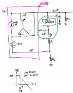
Attachments
Last edited:
You will need to find someone to install that transistor into a series pass voltage regulator simulation. Then you need to have them run the simulation for you, twice. Once with the old (D44H11 bipolar) transistor, and then again with the new (ZXMN7A11) transistor.
You've lost me. (No surprises there. )
)
Breaking the loop as I depicted in LTspice still generates the same operating point as the unbroken circuit.
If I sever the circuit where you have marked Loop Breaker and then pass an AC amplitude of 1 signal (add new voltage source, -ve to ground, +ve to the cap, small signal amplitude = 1) via a tiny capacitor I don't get the correct operating point and V(vout) is garbage. I'm clearly doing something wrong here.
Maybe it is merely a function of the circuit I have been looking at that its AolB declines (immediately) with frequency whereas the Jung/Didden circuit maintains AolB flat for a considerable period?
)Breaking the loop as I depicted in LTspice still generates the same operating point as the unbroken circuit.
If I sever the circuit where you have marked Loop Breaker and then pass an AC amplitude of 1 signal (add new voltage source, -ve to ground, +ve to the cap, small signal amplitude = 1) via a tiny capacitor I don't get the correct operating point and V(vout) is garbage. I'm clearly doing something wrong here.
Maybe it is merely a function of the circuit I have been looking at that its AolB declines (immediately) with frequency whereas the Jung/Didden circuit maintains AolB flat for a considerable period?
How are you generating these (bode?) plots?
Okay, so these are plots of Open Loop Gain vs frequency; Open Loop Gain derived as Vout/Vnfb where Vnfb is the voltage at the inverting -Vin of the op amp.
For my stability analysis I have been plotting Loop Gain or AolB; derived from Vout/Vx where Vx is directly after the injected AC signal and if the AC signal conveniently has an amplitude of 1 then AolB is Vout. I've then been checking phase margin at the frequency at which loop gain is 1, 0dB (with the stability criteria being phase < absolute 180 degrees and a margin from that of at least 45 degrees).
Correct?
If the above is correct then the plots make more sense although the concept of phase does my head in. I get the concept that if x "causes negative feedback to become positive feedback at some frequencies, instability can result" but expressing it in detailed terms of phase becomes as confusing as all hell.
A common mistake people often make, is to forget that the loop breaker must close the feedback loop at DC*.....
In the attached diagram, the AC input signal is applied through Cin
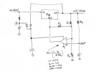
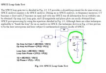
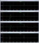
I have read parts 1 and 2 the Tim Green series on Operational Amplifier Stability. He describes in part 2 a process for modelling such in Tina Spice where he breaks the loop with a 1GH inductor and injects the AC signal via a 1GF capacitor (see attached graphic) in order that Tina Spice can find a dc operating point. The approach presented is not dissimilar from your graphic (attached again with highlighting added). However, when I first embarked on checking stability with LTspice, I was told by Helmut Sennewald that the inductor and capacitor were not necessary in LTspice and that the AC signal could be injected into the feedback loop simply by placing the voltage source as I depicted in post #26.
Do you believe this guidance to be incorrect or that I have misinterpreted it? When I posted a schematic in the LTspice forums with inductor and cap Helmut edited to be as in post #26.
Attachments
Besides the Bob Cordell approach and the Helmut Sennewald approach, there is a third approach to simulating open loop frequency response. It goes by the name "Tian probe" and many people here on diyAudio vehemently insist that it is the only righteous, reliable, trustworthy, and accurate-in-all-cases way to go. The Tian probe has the property that it preserves bidirectional signal flow, which might be important if you have no choice but to break the loop at a clumsy place.
I myself have never used the Tian probe method and cannot comment on how easy or difficult it is to implement in LTSPICE. But it seems that many, many people here have done so successfully; inviting the innocent question "how hard could it be?"
If you want a tutor and a coach on the Cordell method, try Bob Cordell. If you want a tutor and a coach on the Helmut Sennewald method, try Helmut Sennewald. If you want a tutor and a coach on the Tian probe method, search around on diyAudio and send out some private messages and/or postings.
I will have to test whether there is a difference between the first two approaches for the following.
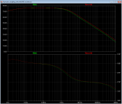
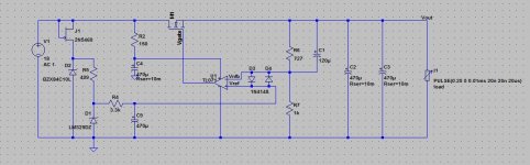
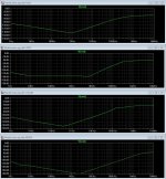
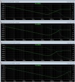
Picking up from the discussion in the super regulator thread, with Mark's kind tutoring I have been looking at Mosfet series pass regulators as I simply could not get comfortable with the stability of the foregoing reg circuits. The basic circuit is presented in the attached graphic. I have modeled four different op amps: TL071, LT1677, LTC1150 and AD797. I also went through a number of Mosfets for the pass transistor. The first 3 op amp scenarios use the same Mosfet while the AD797 seemed better coupled with another.
Presented in the attached graphics (hopefully the screen grabs are legible enough for discussion purposes) are three analyses (1) noise rejection, (2) transient response and (3) loop gain AolB and phase margin.
The noise rejection charts speak for themselves. From not at all bad performance from the TL071 to almost otherworldly (too good to be true?) performance from the AD797. But what about stability?
The phase margin charts suggest 90 degrees of phase margin at the AolB=1 (0dB) frequency and at least 30dB of gain margin when phase hits -180 degrees. Hopefully these tests are valid. How to evaluate the transient responses? The test kicked the load from 0.25A to 5A and back again. While the TL071 seems well-damped, the AD797 settles to the right new Vout considerably faster. Is it appropriate to integrate the error term and choose the one with the lowest error?
Note that the AD797 produces a different Vout from the other circuits. The analysis uses the AD797 model from LTspice's Yahoo Group files section and seems to be an earlier version from Analog Devices. If I use the AD 797A model from Analog Devices' website the error term is worse. I'm wondering about the reliability of these models.
Breakdown voltage for these circuits is high. It comes from three sources that I can see. First the drop across R2. Second, the Vgs required to deliver the load current. This can be observed in the Id versus Vgs curves in the transistor data sheet. Third, there's a limit to the extent to which each selected op amp's output can approach its supply voltage. Do I have this correct?
Attachments
The standard trick for avoiding headroom issues because the opamp's output doesn't swing rail-to-rail, is to insert a DC level shifter between the opamp's output pin and the series pass transistor's control pin (base or gate). Almost all opamps swing their output pin within 2xVbe of their top rail, so a general rule-of-thumb that often works is to make a 4-diode-drop level shifter. Either with 4 diodes, or with a VBE multiplier, or with a zener diode, or with an assemblage of LEDs, or some other equivalent contrivance.
Be sure to heavily bypass the level shifter with a monstrous capacitor, to keep its AC impedance appropriately small. The capacitor also reduces the excess noise contributed by the level shifter. For quick simulation verification an ideal DC voltage source ( ~ 2.5 volts ) would quickly let you see what happens.
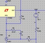
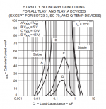
You can of course use a voltage reference IC like the TL431 to implement the level shifter, and get the benefit of its extremely low DC impedance as well. Be sure to choose a bypass capacitor at least 10X larger than the rightmost instability borderline on the datasheet. For the attached datasheet excerpt that would mean 10X 3uF. I'd use at least 100uF. Or you could just select the LM285-2.5 and whistle past the graveyard, since its datasheet displays no stability boundaries. You'd still bypass it with a huge capacitor, of course.
Be sure to heavily bypass the level shifter with a monstrous capacitor, to keep its AC impedance appropriately small. The capacitor also reduces the excess noise contributed by the level shifter. For quick simulation verification an ideal DC voltage source ( ~ 2.5 volts ) would quickly let you see what happens.
You can of course use a voltage reference IC like the TL431 to implement the level shifter, and get the benefit of its extremely low DC impedance as well. Be sure to choose a bypass capacitor at least 10X larger than the rightmost instability borderline on the datasheet. For the attached datasheet excerpt that would mean 10X 3uF. I'd use at least 100uF. Or you could just select the LM285-2.5 and whistle past the graveyard, since its datasheet displays no stability boundaries. You'd still bypass it with a huge capacitor, of course.
Attachments
You've lost me there, care to explain what you're doing, where exactly is x on the sheet? (or simply post the .asc).
For my stability analysis I have been plotting Loop Gain or AolB; derived from Vout/Vx where Vx is directly after the injected AC signal and if the AC signal conveniently has an amplitude of 1 then AolB is Vout.
Hi Elvee, see post 26. It shows where the AC signal is injected and where X is.
PS: this is a good video to watch as well Solutions - LTspice IV: Stability of Op Amp Circuits
PS: this is a good video to watch as well Solutions - LTspice IV: Stability of Op Amp Circuits
The level shifter is (Q2 + D2). Q2 ensures that D2 gets at least 5mA of bias current, at all times, whether the regulator output is lightly loaded or heavily loaded. Q2 is sized to provide (max(Ib(Q1)) + 5.5mA) across all variations in temperature, input voltage, and component tolerances.
Notice that the level shifter's bias current must come from Vin_unregulated. Vout_regulated is too low.
Notice that the level shifter's bias current must come from Vin_unregulated. Vout_regulated is too low.
- Status
- This old topic is closed. If you want to reopen this topic, contact a moderator using the "Report Post" button.
- Home
- Amplifiers
- Power Supplies
- Adventures with 5A regulated voltage circuits