Thanks for reply.Nothing special.. Loopback, signal from card output to amp, signal from amp output to card line input , via voltage divider at low impedance. Normal shielded cables, shield always connected at both sides.
It is good to find optimal level for card input / output for minimal distortion, and than keep signal near this level, if possible.
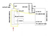
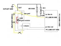
And I found basic mistake in all posted schematic here. If an input ground, isolated from power ground via 10R resistor (ground loop currents limit ) should have any sense, than grounded end of NFB resistor must be connected to this input ground (junction R2,C2,R3), not to power GND. Other way this 10R resistor only worsens mains artefacts.
For CFA amp (NFB resistor only 50R) decrease value of R3 to 1-2.2R, but best solution is not to use this resistor at all (replace with jumper to power GND).
For CFA amp (NFB resistor only 50R) decrease value of R3 to 1-2.2R, but best solution is not to use this resistor at all (replace with jumper to power GND)
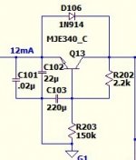
That is the reason why this yellow wire added ,by-passing this lift gnd resistor
Attachments
Last edited:
Do not use "special" wire direct to star gnd point, it is not good.. Simply replace 10R resistor with shortest wire jumper (cutted resistor lead ) instead of 10R, at the same place. Input GND and input bias resistor (10k) ground side should be at the same potential as NFB return path ground (ground side of 50R). Traces at PCB are not zero impedance, so I recomend GND as poured copper plane.
Ok understand this.Do not use "special" wire direct to star gnd point, it is not good.. Simply replace 10R resistor with shortest wire jumper (cutted resistor lead ) instead of 10R, at the same place. Input GND and input bias resistor (10k) ground side should be at the same potential as NFB return path ground (ground side of 50R). Traces at PCB are not zero impedance, so I recomend GND as poured copper plane.
The recommendation is about direct ground input point with a short link instead of this 10R resistor.
I will try this soon.
Thanks again.
Attachments
Last edited:
I'm having mixed success with the CFA mod at the moment and comparing with the simulated version to try and make some sense of what I am seeing.
Thimios, I tried using the 10R thingy in the wolverine but it didn't work so well so I completely removed it. The point of the resistor is to attempt to keep currents out of where they don't belong, keeping it in, I presume, means your internal wiring can be less 'correct', but it created issues for me, so I just did the wiring correctly and bye bye issues.
Thimios, I tried using the 10R thingy in the wolverine but it didn't work so well so I completely removed it. The point of the resistor is to attempt to keep currents out of where they don't belong, keeping it in, I presume, means your internal wiring can be less 'correct', but it created issues for me, so I just did the wiring correctly and bye bye issues.
Member
Joined 2009
Paid Member
Traces at PCB are not zero impedance, so I recomend GND as poured copper plane.
If only it were that simple. Ground plane has to be carefully used as high frequency signals don't just flow into the ground plane, they follow paths through it and you can be worse off than a simple trace.
Well I am making some progress. Thank you BV for the additional component changes as these helped.
I have now successfully got the thing to bias correctly, at least it appears to. This is using a micro controller controlled variable resistor from AD. It's rather nice setting the bias with the push of a button and rather more consistent than tweaking a pot, although not infinitely variable like the mechanical counter part.
I am still getting offset, but that's trouble for another day.
Briefly though I am able to adjust the two trim pots to set the current across R13 and R14 so that they match, but the currents across R15 and R20 are not equal, nor are the currents across R16 and R21 equal. There is very little DC present at the bases of the input pair when referenced to ground.
I will fire the thing up again on the 25volt PSU tomorrow and see if that changes things, but from simulation it doesn't appear to. In simulation it works perfectly on 9v rails.
I am assuming that when one sets the amplifier up and balances the currents that you do this until the voltage drop across R16 and R20 = 1.67mA flowing through them?
If you have a second bench PSU connect these in series. I make this every time when i do a first test to a diy amplifier.
Most of my INP haven't matched pairs except inp trans.
Indeed, I've been meaning to either buy a second higher voltage unit or build something for the few times I actually need more voltage. The supply I've got goes upto 19V but will output ≈10 amps, which has actually been quite useful for some stuff. You can't have it all. But if I were to build a boosted split supply at least I've got something beefy to power it from

It is unimportant (equal currents R15, R20), the only what counts, is DC zero at output ( than should be voltage across R15 and R20 nearly equal, and the voltage across R16 and R21, too. )to set the current across R13 and R14 so that they match, but the currents across R15 and R20 are not equal, nor are the currents across R16 and R21 equal.
Input pair imbalance(and internal stages unsymetry) is compensated using slightly different currents via both halves (different setting current sources Q3,Q4).Only if everything were perfect, than were voltages and currents symetrical, too.
Can you exact specify what components you mean?some of the "mods"
If only it were that simple. Ground plane has to be carefully used as high frequency signals don't just flow into the ground plane, they follow paths through it and you can be worse off than a simple trace.
Ground planes shouldn't replace star grounding and intelligent bus grounding schemes, only supplement for improved parasitics and shielding. At audio frequencies a ground plane might even carry interference from the output stage to the frontend - I think a partitioned ground plane is a better idea.
One idea for using a ground plane is to connect the plane to a star ground in only one place. This way, any current loops within the area of the plane will be magnetically shorted and have low inductance, radiation and magnetic interference. At audio frequencies however, high currents may cause current to spread out across the plane and interfere with other traces. This is much less if there is only one electrical connection to the plane, which means there will be much less currents which aren't magnetically induced in it and following the path of magnetic coupling.
As I understand, signals radiated from the ground plane into a parallel trace will occur at frequencies where the inductance of the ground plane is swamped by its resistance. In the resistive frequency region of the ground plane, the currents will no longer follow the path of magnetic coupling and will instead spread across the ground plane following the path of least resistance, and the magnetic field resulting from this will couple into other traces on the board.
A 1oz copper ground plane of 10cm x 10cm based on my calculators has an inductance+resistance corner frequency of around 5KHz - so it is safe to say that at audio frequencies, a ground plane can't help magnetic radiation much. The output stage generates enormous currents, so I think it's plane should definitely be partitioned.
Return path for high currents (e.g. speaker ground terminal to PSU GND point) must be low impedance and as short as possible. It is part of correct PCB design, to split ground plane to more segments, connected together in one correctly selected point.high currents may cause current to spread out across the plane and interfere with other traces.
It is unimportant (equal currents R15, R20), the only what counts, is DC zero at output ( than should be voltage across R15 and R20 nearly equal, and the voltage across R16 and R21, too. )
Input pair imbalance(and internal stages unsymetry) is compensated using slightly different currents via both halves (different setting current sources Q3,Q4).Only if everything were perfect, than were voltages and currents symetrical, too.
Can you exact specify what components you mean?
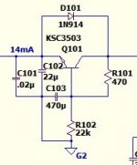
The OPS has a cap multiplier built into the board that drives the IPS. The original used 470R/22K voltage divider. Both you and OS changed that in your mods for the IPS. My question is whether or not that is an important part of the mod? I thought the idea of this modular design was that we could build the OPS and use as is, and simply attach different types of IPS modules. I don't want to have to modify the OPS every time someone comes up with a new IPS. Defeats the purpose IMO.
Attachments
Last edited:
2 still4given
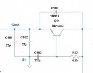
Target of all this modifications was to improve PSRR, that is why here are cap multiplier modifications. Simply calculate time constant (RxC) of colector to base resistance and capacity from base to ground. If multiplier transistor has high enough h21, you can use larger value for resistor and so increase time constant - improving filtration. At the same time voltage drop across multiplier should remain reasonably low (2-3V), so exact values depends on transistor parameters. Here is no need to change this for other IPS in use.
2 bimo
first sight - Q107, Q16 allowed Uce=230V, transistors are exposed to full PSU voltage- 280V, the same diodes D22, D23, they should be rated at least for 140V and more. For switching to high voltage PSU rails is better to use Mosfets (something like IRFB4228 for both polarities ) instead of paralleled bipolars.
The BC3x7-40 would be the best transistors for the C-multiplier. Put a diode or two across the base-feed resistor to make sure Vce never exceeds more than a few volts. The BC3x7 is extremely robust and can handle up to 1A inrush surges, so as long as your frontend reservoirs aren't too large, it can fill them instantly.
I modified spooky-amp into class H. Please comment.
I do not have experienced to build such high power amplifier, but I want to learn.
hey.. sir bimo, i try to see your simulation but i cannot find some component for tr model, can u give component to run this simulation?
Putting diodes across base resistors will also dramatically increase BC3x7 base currents at switch on , and I am afraid, that BC3x7 can not reliable survive this for long time..The BC3x7-40 would be the best transistors for the C-multiplier. Put a diode or two across the base-feed resistor to make sure Vce never exceeds more than a few volts. The BC3x7 is extremely robust and can handle up to 1A inrush surges, so as long as your frontend reservoirs aren't too large, it can fill them instantly.
hey.. sir bimo, i try to see your simulation but i cannot find some component for tr model, can u give component to run this simulation?
I use model from Cordell and Keantoken. May be I change the name. Please use these.
Attachments
2 bimo
first sight - Q107, Q16 allowed Uce=230V, transistors are exposed to full PSU voltage- 280V, the same diodes D22, D23, they should be rated at least for 140V and more. For switching to high voltage PSU rails is better to use Mosfets (something like IRFB4228 for both polarities ) instead of paralleled bipolars.
May I use MJE15034 and MJE15035 for Q107 and Q16?
D22, D23 I will use 1N4007.
Can you share schematic switching to high power supply using mosfet?
MJ15035/35 are sufficient from Uce wiev. 1N4007 is too slow, use e.g BAV21.
I have not complete schematic to switching PSU rails available, but it is often used in class H PA amps (e.g QSC RMX2450), many schematic and service manuals are available on web. Try to search inspiration here.
I have not complete schematic to switching PSU rails available, but it is often used in class H PA amps (e.g QSC RMX2450), many schematic and service manuals are available on web. Try to search inspiration here.
Last edited:
- Home
- Amplifiers
- Solid State
- Slewmaster - CFA vs. VFA "Rumble"