No one is disputing what works for some and not for others, this thread is intended to produce a result that EVERYONE can duplicate.
Sorry but that's an unrealistic goal.
There´s no task that absolutely *everybody* can do well.

Not *everybody* can play guitar/ride a bicycle/swim/type/whatever yet there are millions who can.
Personally , although I silkscreen for series production and have used all other methods (including positive and negative photo emulsions) , also *have* mastered the toner transfer without resorting to mystery papers, just raw coated printing ("magazine") paper.
As in everything else, practice makes perfect.
And an *important* point is accurate temperature, which by the way is not "maximum" .
I bought a secondhand clothes iron a long time ago, experimented until I got the right temperature and marked the thermostat knob.
Temperature is very important because too cold does not adhere to copper and too hot melts too much, smears, and much worse, being so liquid it gets absorbed back into the transfer paper pores (even coated there are some) and then you can´t pull it away, no matter how much you soak it.
I have never tried the solvent processes, thermal is much more controllable.
The beauty of thermal is that from on monitor screen to etched PCB it can take as little as 30 minutes, go figure.
A friend asked me yesterday for an RIAA preamp so he transfers his Vynils to MP3 and a "Fake Alarm" Led blinker for his car, will make both in less than an hour.
No, not as nice as photo transfer , edges are not as clean cut, but so what ?
Remember, uniform temperature and pressure is the key to success.
Any method that requires repeatability is a dead duck. It might be OK for really coarse PCB layouts but its hopeless with fine tracks and pads.
The photo method is very reliable and is easily achievable with the minimum of outlay.
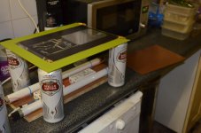
I do giggle at the guys that spend £100's on a UV exposure box. My exposure box consists of 2 x UV tubes (OK proper wavelength ones but still only £3 each) with electronic ballasts (£5 each from Ebay). The exposure table is a piece of glass balanced on 4 x large beer tins. (empty of course).
The photo film is available on E-Bay for about 50p a sheet or from Germany at £8 for a metre (that goes a long way if you buy 2m)
The developer is peanuts.
I've used all of my printers to produce a photo image and all have worked, you only need tracing paper which is also cheap.
If you look closely you will observe that this method requires a photo negative of the PCB, ie the tracks are blank.
The photo method is very reliable and is easily achievable with the minimum of outlay.
I do giggle at the guys that spend £100's on a UV exposure box. My exposure box consists of 2 x UV tubes (OK proper wavelength ones but still only £3 each) with electronic ballasts (£5 each from Ebay). The exposure table is a piece of glass balanced on 4 x large beer tins. (empty of course).
The photo film is available on E-Bay for about 50p a sheet or from Germany at £8 for a metre (that goes a long way if you buy 2m)
The developer is peanuts.
I've used all of my printers to produce a photo image and all have worked, you only need tracing paper which is also cheap.
If you look closely you will observe that this method requires a photo negative of the PCB, ie the tracks are blank.
Attachments
Last edited:
How about a direct print trace method ?!!!!!!
This is something that I have been hoping would come along soon and it is now finally here !!!
https://www.kickstarter.com/project...nting-circuit-boards-with-home-print?ref=live
I would imagine the Ribbon Speaker DIYer's would love this !!!
jer
This is something that I have been hoping would come along soon and it is now finally here !!!
https://www.kickstarter.com/project...nting-circuit-boards-with-home-print?ref=live
I would imagine the Ribbon Speaker DIYer's would love this !!!
jer
I just don't see the problems....... KD- a 10£ (?) lamp fixture for those tubes should be easily available. Add a few spacers, pieces of wood, beer cans ( maybe a bit tall ? ) and a piece of glass, and - voila, - you have an exposure unit.
Most newer laser or ink jets should print with sufficient density on transparencies, at least for simple boards. For fine line work some special media is well worth the ' not so much money'.
Positive coated boards are sold by most parts vendors, and are quite cheap these days. For negative boards, you either need a reversal film, or do a reverse print, which in my experience can give problems with ink fill as the areas to fill wil usually be larger. As far as I know, negative boards are also more expensive.
Developing can easily be done with regular caustic soda, - I've made boards with .625 mm pad spacings with soda, - with no problems. Cleanliness and proper care and accuracy is needed for a good result.
Just pointing a detail:
*If* you decide to go the negative resist path, , which requires a negative PCB print (it was correctly noted that getting deep uniform black in wide areas is problematic) , you are halfway towards the silkscreen process. Why?
1) you will also use a couple UV tubes , a sheet of glass and something to press negative together. *check *
2) you'll need a transparency or tracing paper print. *check*
Which by the way is positive (easier) because the silkscreen itself *develops* negative and will *print* positive.
3) you will still have to develop, in this case the screen emulsion (instead of the PCB emulsion) *check*
4) well, this one is extra: you will have to mix and apply emulsion.
Which by the way is easy to do right: you apply a couple spoonfuls on the screen and spread it on both sides with a schoolkid plastic ruler.
It's uniform by definition, because you spread it in all directions and lift excess (with the same plastic ruler) so only remains "what the cloth takes" .
Yes, you have to let it dry in the dark or subdued light (no fluos or CFL pleas, just a plain old 40 or 25W filament lamp, clear or coloured (yellow is best).
5) you screen the resist ink on the PCB.
The beauty is that there are different types, all are much better than any emulsion, one of them is very easy to pull afterwards with a spoonful of caustic soda (sodium or potassium hydroxide, which you but at the hardware shop) or simply wipe away with some solvent or brush away with steel wool and water.
I have done it for just one PCB, go figure, although now prefer the iron on transfer.
And if you need many (say 8 preamps for a mixer or a PSU which you will use in many projects or want to share PCBs with friends or colleagues), for the first one it takes a little more than a regular photo sensitive PCB but then any extra copy (in the same session) takes extra 30 seconds, how's that?
Not trying to convince you to do that now, but consider it in the future as a possible alternative.
Which if mastered will also let yopu apply solder mask, component screen printing (duh!) and front/back chassis panel graphics and lettering.
Plus some tasty Lab/Band/Event T Shirts
Or decorate/label amps, cabinets, road cases and drums.
A skill well worth learning
The reason that I am opting for the photo negative film is mainly down to how much failures cost.
The photo negative film is only £1 a sheet (B5). As you only need to buy common clad board the cost per board is initially lower. And, if you have a disaster you can wash the bad photo off the board and try again.
The photo positive boards could be re-prepped but the spray cans are next to useless and I haven't found anyone supplying photo positive film.
The tools and chemicals for both positive and negative all cost about the same.
Both methods require a decent opaque image which most 1220dpi lasers, inkjets and inkgels can achieve.
You can have a hole in a trace as much as you can have a hole in a fill pattern, I've not had this issue with my inkgel printer. An excess spot of copper on a finished board is easier to deal with than a hole in a track.
As for the beer cans, they are actually too short. The negative photo resist needs an exposure at about 12" (300mm) and for only a few seconds, (Depending on the film used - I use 3-6 secs).
Last edited:
The only choice for get photo positive film is diapositive film. Extremely hard to find in this digital era.
Could you make a resume with the goals and the findings until this moment with a cook book of the best kind of method for make pcb in the kitchen?
I think or suppose that when I get the better system I will concrete many of my dreams and projects. I think the pcb is the easiest, clean and reliable form in DIY electronic and until nowadays I never reach the goal. Thanks KatieandDad and gentlemen.
I'm not sure where you get the idea that the photo negative film requires the adding of an emulsion.
It uses the same technique as the photo positive boards. The only difference is that the printed image is a negative and the UV light is curing the photoresist. It is then developed washed and etched exactly the same as a photo positive board.
It uses the same technique as the photo positive boards. The only difference is that the printed image is a negative and the UV light is curing the photoresist. It is then developed washed and etched exactly the same as a photo positive board.
Fahey are you asking about a photosensitive emulsion for use in silk print for t-shirts?, You print first in a transparent film and put it between a source of light (UV) like a mask, Later you develop the bcbcard that's is now print on the copper. The process continues the same in acid or ferric perchloride.
Sorry about the misunderstanding.
The process with the negative film is also very simple, the beauty is that you can re-apply the film if you make a mistake.
1. Take the photo negative film and cut it to size.
2. Clean the copper clad board with fine abrasive paper and wipe clean with mentholated spirit.
3. Peel the thicker film off the photo negative film and apply the film to the copper board carefully removing any bubbles of air.
The film can be lifted and reapplied without any problems at this stage.
4. Pass the board through a laminator or iron it with a moderate iron to set the emulsion onto the copper.
5. Expose the board with a photo negative with a UV light source.
6. Remove the upper film from the photo resist.
7. Now you can etch it in the normal manner with Ferric Chloride (or the etchant of your choosing).
8. The film peels off easily after soaking in a caustic soda solution.
Hi friends.
After many unsuccessful methods i have solved the problem "home made pcb"
Here are all details see post #1152 .http://www.diyaudio.com/forums/solid-state/221741-dx-blame-st-together-dx-super-116.html
All my diy amplifiers built with this method.
Thimios.
It seems that no one believes me!
100% repeatable results ,no fails ,no more bad pcbs.
Thimios.
your old link took me to post1401 by still4.It seems that no one believes me!
100% repeatable results ,no fails ,no more bad pcbs.
Thimios.
Where should the link take me?
Everything about homemade pcb explained here :http://www.diyaudio.com/forums/solid-state/221741-dx-blame-st-together-dx-super-116.html
post#1152.
Regards.
Thimios.
post#1152.
Regards.
Thimios.
Last edited:

No-one is trying to say which method is better, it would be nice to just find a method that is suitable for each individual.
Each has its drawbacks, some are more reliable than others.
Thanks to E-Bay the iron on Photo Negative film method is now very cheap, very reliable and repeatable.
Each has its drawbacks, some are more reliable than others.
Thanks to E-Bay the iron on Photo Negative film method is now very cheap, very reliable and repeatable.
Last edited:
- Status
- This old topic is closed. If you want to reopen this topic, contact a moderator using the "Report Post" button.
- Home
- Design & Build
- Construction Tips
- Home Brew PCBs