I agree there is no need for the "grounded" RC network. BTW it's not a "Zobel" in the true sense of maintaining a resistive load at all frequencies.
Most people call it a zobel, but I guess we could call it a snubber.
I simulated this circuit to make sure it worked before uploading.
I captured it the best I could in ltspice and made it work. Kind of. But it works only with a 4ohms load, for a reason I don't yet understand. When I put an 8ohms or even 5 or 6 ohms load, it doesn't give a sine wave coming out, just a small fraction of a wave and that's it. Bizarre.
After trying a few things, I was able to push it to obtain a full sine wave of the output with a 120V peak to peak. So it is actually bridging, and must be swinging that power supply around the ground to provide this, as the "low side" output is indeed grounded.
However, I am not yet getting the low thd you mentioned, perhaps because of the models and the different choices of some parts. Plus I added a current source with a zener and a transistor on the input ltp stage (about 2mA)
I agree R37 and R46 may need to be checked that they don't run into trouble with floating PSU's. Might be a good idea to have a centre tapped PSU connection for these.
That's what I was thinking, because when the ground swings close to the + rail, then those transistors above are reversed biased aren't they?
Wouldn't it be sensible to aim for the opposite rail instead of some intermediate level near ground?
If we can avoid a psu with a center tap, all the better, as that is one of the main features of the grounded bridge, it's supposed not to need a center tap and the psu can be made simpler with filter caps between rails. Of course they need to be handling twice the voltage, but we use half their numbers and much less wiring. And in this case, it's no huge deal to find higher voltage caps, as we're only aiming for +-35V rails, so 80V filter caps can be suitable and can be found.
Q4 and Q5 servo the currents in the CCS for the VAS stages. If these were not accurately balanced for the currents in the VAS transistors the outputs would drift up or down depending on who pulled harder.
I see, I figured something like this, more or less, but I prefer having your full explanation.
Can we make it without any center tapped psu? with only one voltage source?
We could make a divider to obtain that middle point reference (for R11), since there is no need for any current handling.
I made the current source for the input ltp with the bias resistor hooked to the opposite rail, which works fine. This avoids needing to aim at ground.
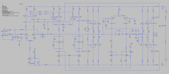
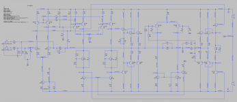
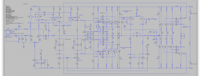
I'm attaching my ltspice sim file and models files used. So we can correct and tweak it properly. I used the ltspice models from its library for the small signals (BC546/56B), but it might be good to use the BC550/60C at least on the input diff amp, and perhaps current sources and mirrors, if the Vceo won't be an issue. There are quite a few BD139/40 and I see the bias currents are fairly high in the vas stages compared to most setups, so I guess they're not overkill and could eventually be heatsinked, perhaps all the vas and bias spreaders for each side could be put together on the same heatsink with the drivers, separate from the TO3s... Do we need to track the TO3's heat or can we just sense the drivers?
With only 2 pairs of outputs on each side, I don't think a 4ohms load on the bridge would be a good idea. Although a proper soa limiter protection could prevent damage, while making itself heard with higher distortion.
In the models file for the sim, I added models to try later.
There is one thing I don't understand though: The gain seems to me to be close to 30, and I expected to be able to get full output swing for much less input. I had to use 3.8V peak on the inputs to get the near full power (about 400W/4ohms) swing on the output, which is close to 120V peak to peak. I thought it would take far less than that with such a gain, or perhaps I'm miscalculating the gain.
I biased the output stages for about 100mA per transistor, which should be handled properly with good heatsinking.
Now if we could lower the thd at 20khz somewhat, that would be perfect.
Attachments
I agree R37 and R46 may need to be checked that they don't run into trouble with floating PSU's.
I tried different things (sims), using other models for the 3055s, namely the MJ15015/6, which are basically the same thing but they're "supposed" to be complementary, and perhaps the models are ok (or not). Having tried other amps with those models, it appears they may be ok, but I wouldn't know for sure until they're fully checked out.
There is one thing that I found out that requires some checking. Because after trying those other models, and also trying to send R37 and R46 to the opposite rail instead of ground (with higher res values), and then removing those changes to make sure, the amp exhibits a behavior that is cause for concern.
What happened is that when I tried it before, I didn't put an input signal too strong to keep it below clipping, so it worked properly, apparently, and your simulation may also have worked out that way. However, what started this is when I used the other models (MJs), perhaps they had higher gain, or something a bit different from the 3055 models used at first, the output signal wanted to get bigger, but didn't just clip normally, it was just a small partial wave form and no real signal. Maybe the amp sticks to a rail or something like that, instead of just clipping.
At first I just couldn't figure out why that was happening and I figured the amp didn't work at all and I pulled back the changes. Well, with the original models and setup, it actually does the same thing when we increase a tiny bit the amplitude of the input signal. This was also happening when changing the load impedance, because the amp was working just fine with 4ohms load, but would behave badly on 8ohms, and finally it would also stop working even on the 4ohms load.
Reducing the input signal amplitude makes it work again, so that's happening at clipping. I doesn't take much, for example I was getting the bad behavior with a 1.36V input signal, and then lowering it to 1.35V made it work again.
Pulling up to rail R37 & R46 didn't help that, but still, I believe they should be hooked in an other way than to ground. More sims are needed.
Did you try baker clamp?
Here are some sims using the circuit with the "grounded" resistors discussed taken to the centre tap of the floating PSU. I get 192W into 8 ohms and no problem with clipping (300W).
Usually strange behaviour is due to oscillations. Try increasing the sprog. stoppers or adding a small resistor in series with the global feedback resistors or if necessary 220pF across the bases of the pre-VAS transistors (to Vdd).
John
Usually strange behaviour is due to oscillations. Try increasing the sprog. stoppers or adding a small resistor in series with the global feedback resistors or if necessary 220pF across the bases of the pre-VAS transistors (to Vdd).
John
Attachments
Here are some sims using the circuit with the "grounded" resistors discussed taken to the centre tap of the floating PSU. I get 192W into 8 ohms and no problem with clipping (300W).
Perhaps I'm not reproducing the simulation 100% properly, or perhaps ltspice isn't behaving like an other simulator. I get consistent result, so something must be different.
At first I was getting a ~ 120V peak to peak output sine wave, and that was with a 4ohms load and the models I used at first. This odd behavior showed up when I tried an 8ohms load, but I didn't know what was going on and didn't know the amplitude of the input signal had an impact. I just found that the output signal was not a sine wave. Going back to 4ohms load made it work again, at that time.
Then when I switched to other models, things changed a bit and I found out the input signal amplitude needed to be reduced to make it work again, although with a lower power output.
Usually strange behaviour is due to oscillations.
That's what I was thinking, so I did a lot of experimenting with the compensation, with values going rather large, but didn't fix the issue. Although I'm sure I haven't tried everything and probably not the best method.
Try increasing the sprog. stoppers or adding a small resistor in series with the global feedback resistors or if necessary 220pF across the bases of the pre-VAS transistors (to Vdd).
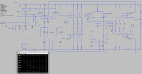
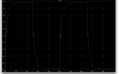
I will try a few things, and in the mean time, I'm posting the schematic used for simulation, and one of the output screenshot shows an output sinewave signal, which is generated with an input signal at .9V, and then the non sine wave output signal is obtained with the input at .92V.
I had wrongly evaluated the input signal amplitude previously, so I thought it would take a large one, but I revised the way the sources and their parameters are set up.
I'm trying again increasing the values of C1 & C4. so far 100p doesn't change anything. I also just added 2 caps, 220p from the bases of Q10 & Q9 to the V+ (I assume that's what you meant by Vdd). And at the moment, the behavior is still there.
Attachments
Ok, trying various things, with added caps (C12 & C15), higher values for C1 & C4, as well as C9 &C10, also played with C2, C3 and even C6 & C7, just in case. Tried adding resistors in series with C9 & C10, and nothing has worked so far.
The higher cap values change the gain (the sim freq is 20k), so the increase of input signal amplitude needs to be higher to come to the point when it no longer works. But the behavior is there.
I may have omitted something, connected something wrong, bad value, something that causes this, but I didn't find it. Perhaps someone will catch the eventual error, but I checked many times over and couldn't find a mistake. Other eyeballs need to peer at this...
I'm posting the ltspice sim file and the models file used.
Attachments
I've been thinking about the protection and what the VI limiters do. Although VI limiters prevent SOA violations (if properly calculated) and will protect against overloads, they won't protect the speaker in case of amp failure and a rail goes out to the output.
Since the relays can't be trusted to handle high current DC in catastrophic situations, the speaker could be at risk if the relay's contacts fuse.
This brings me to think about the solid state relays, and if one of those can be on the amp's output, plus one on each rail (after the big filter caps), then the vi limiters are no longer really needed.
There really should be a good protection for the speakers, not only the amp itself.
The solid state relays don't cost that much compared to good mechanical relays and if the vi limiters are removed, that's fewer parts and cost from there that can be shifted to the solid state relays. So in the end it might be that we can have a better overall protection without much additional cost.
Solid state relays don't take up much room and could be right on the pcb in the best spot. They don't even need heatsinking, so it's easy to put them where needed.
This could in fact simplify the amp circuitry itself, as the part count might be lower, and a benefit would be sonics, if vi limiters are not there to pollute.
Though I am thinking it might be a good idea to think about a clipping prevention. Perhaps some way to compress or limit the input signal, so the amp can never be driven into clipping. This may be feasible with opamps...
My goodness. What poor models you are using. Early voltages of 30 and 10 for the 2N3055 and BD140?
I wondered about the use of 2N3055A rather than 2N3055 but the tF for 2N3055A and MJ2955 are both 10nS. I'm surprised you get any good results at all. What appears to have happened is that ON Semi must have contracted MODPEX to produce models of their devices. MODPEX used worst case limits and haven't provided typical models, in my opinion. So the model will guarantee that you get high leakage currents at (say) 60V (the rated ICEO for example). BUt in practice as mentioned several times the 2N3055 offered by OnSemi and ST typically have BV's of over 80V and therefore TYPICAL values of early voltage won't be anywhere near as bad as worst case leakage specs. say. For true modelling we need best, typical and worst case models representing actual manufacturing tolerances.
I'm surprised Philips have a model value of VAF of 10 V for the BD140. One of the key attributes of these devices was that they performed better than old TO-5 counterparts (e.g. BFX84). I have to say I use my own model parameters reflecting measured Early voltage (around 120V or so BTW) for these devices. I haven't released them generally because I haven't fully validated them.
My goodness. What poor models you are using. Early voltages of 30 and 10 for the 2N3055 and BD140?
That would not be surprising. That is why I wish we had a good repository of known good models.
I have been using models from keantoken, but I didn't get a 3055 model, so I'm using the ones I found, mostly from onsemi. I've tried several, but I don't know which is best.
I need to double check which bd140/139 I am using, because they are present in bob cordell's collection.
I wondered about the use of 2N3055A rather than 2N3055 but the tF for 2N3055A and MJ2955 are both 10nS. I'm surprised you get any good results at all. What appears to have happened is that ON Semi must have contracted MODPEX to produce models of their devices. MODPEX used worst case limits and haven't provided typical models, in my opinion. So the model will guarantee that you get high leakage currents at (say) 60V (the rated ICEO for example). BUt in practice as mentioned several times the 2N3055 offered by OnSemi and ST typically have BV's of over 80V and therefore TYPICAL values of early voltage won't be anywhere near as bad as worst case leakage specs. say. For true modelling we need best, typical and worst case models representing actual manufacturing tolerances.
I did get a big collection of modpex models, and I use them when I can't find anything else.
Where could I get a good 3055 model then?
I did get fairly good results in sims with 3055s so far, even much better than mj15003/4 on a leach amp sim. I was able to bring thd to 0.00xxx levels in 3055 sims, with the models I have on hand.
I'm surprised Philips have a model value of VAF of 10 V for the BD140. One of the key attributes of these devices was that they performed better than old TO-5 counterparts (e.g. BFX84). I have to say I use my own model parameters reflecting measured Early voltage (around 120V or so BTW) for these devices. I haven't released them generally because I haven't fully validated them.
I will double check which models I have used. Those used by keantoken might be better than those philips.
Perhaps once we get this repository of known good models going, you'll be able to share some as well. Collaborative work can be it easier to verify models.
I switched some models and I made a sim with the MJ15015/6 (3 pairs) as the 3055/2955.
The bd139/40, mje15032/3 and bc550/60 are from bob cordell's collection.
The mj15015/6 models are from onsemi.
Regardless, I am still experiencing that issue when upping the input signal to get closer to max power. I can reach an output amplitude of about 100V peak to peak, which is even less than what I got before. This is about 35Vrms, a little more than 150W/8ohms.
In this sim as it is right now, the input signal is set at 0.83V (peak), and if I up that to 0.84 or above, then the malfunction happens. What could be causing that? It will not reach clipping, not even close.
Attachments
I don't know what the problem is but I do not see it in my simulations. My sims clipped at +/-60V which is interesting for a 2N3055/MJ2955 pair. Does LT spice take account of breakdown voltages in the transistors - if so perhaps there is one which is sailing close to the wind. Try BC556/BC546 or 2N5551/5401 for example just to check.
Sometimes mysterious clamp voltages occur if a current source stops being one - if a bias condition suddenly reverses. This can happen if a transistor saturates or something similar. Try swapping current sources and use voltage sources for some of the bias gens. perhaps.
Sometimes mysterious clamp voltages occur if a current source stops being one - if a bias condition suddenly reverses. This can happen if a transistor saturates or something similar. Try swapping current sources and use voltage sources for some of the bias gens. perhaps.
I don't know what the problem is but I do not see it in my simulations.
I suspect you're not using ltspice, so there must be some difference.
My sims clipped at +/-60V which is interesting for a 2N3055/MJ2955 pair.
Curiously, I did get the same thing at first, and that was nice to see, as the sine wave was clean and the thd somewhat decent already at 20khz.
But since that I never could reproduce it, it's been doing this. For a while it was a little below clipping, or perhaps so I thought, but in all the different sims with various transistors that I've tried, it's been consistent and working fine up to about 50V peak (Vout), and then anything above that malfunctions.
Does LT spice take account of breakdown voltages in the transistors
That would be nice, as it would be that much closer to reality, but I suspect not.
- if so perhaps there is one which is sailing close to the wind. Try BC556/BC546 or 2N5551/5401 for example just to check.
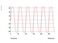
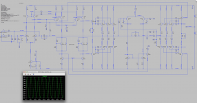
Alright then, that's a track to follow. So I tried first to replace all the 550/560 with the 546/56 that come in ltspice's library. No success with that. So then I replaced all the bc small signals with the 2N5401/5550 that are in the library as well. And here again, the exact same thing, at the same output level.
I took screenshots of that, attached...
Sometimes mysterious clamp voltages occur if a current source stops being one - if a bias condition suddenly reverses. This can happen if a transistor saturates or something similar. Try swapping current sources and use voltage sources for some of the bias gens. perhaps.
Good idea. I'll try some things now...
Attachments
Try swapping current sources and use voltage sources for some of the bias gens. perhaps.
You were really on to something there.
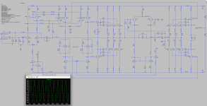
I figured the best place to start would be the CCS for the input diff amp, so I put a spice CCS instead of that discrete transistor plus zener one, and sure enough, I could drive it higher.
I tweaked this a bit and was able to drive it all the way into hard clipping without that odd behavior happening at all.
So it definitely was that type of CCS that wasn't suitable.
Then I figured I would try on a different type of CCS, so I put the dual transistor type, just like the other one was, but this time, no zener, and that one works perfectly.
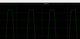
You can see on the screenshot that I gave it 1.25V input and it's clipping pretty hard now.
The second screenshot shows the detail of the positive end clipping. Isn't there something that looks similar to a slight overshoot? Perhaps some compensation adjustments could help that get smoother.
Now I can try adding a vi limiter. Only on the left side would suffice (high side).
Attachments
Since the different current source is working better, I was able to test a few more things and I added a vi limiter. For now the values in the limiter don't let it act at all, so it's not really there and it doesn't interfere. We'll calculate values for that later.
I tried an other model of the 2n3055 and curiously the thd went down, although I had to make a huge bias adjustment for that one, so there are big differences between those models, and it would be good to have a reliable one that's as close to real as possible.
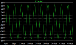
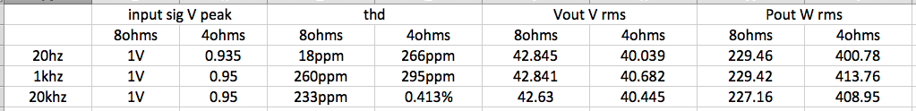
Clipping happens a little above 60V peak, so I keep the drive level to stay below clipping and with a 1V peak input signal, we get a bit over 42.6Vrms (~226W) on 8ohms load, and hardly less on 4ohms, so the power doubles. I know the real psu will sag, and I added a serial resistance to the power sources of 0.25ohms, to make it a bit more realistic. I may be conservative though, the real one may be worse, but that will depend on the transformer choice mostly.
I put 60mF of filter capacity on the sources as well.
The thd on 8ohms at 20khz at that drive level is at 233ppm and it goes up to a little over 0.1% on 4ohms.
I tried the square wave and looked at the slew rate, which I think it around 20V/us.
This ain't bad at all for 3055s.
The thd at 1khz on 8ohms goes down to about 26ppm. Real nice! On 4ohms, we get the effect of the psu sagging, so it clips at that same drive level and the thd climbs. But lowering the input signal to 0.95V brings it out of clipping and the thd drops to 295ppm and the power is still a bit above 413W.
The key is a stiff psu to get the most out of it.
I'm not seeing any signs of oscillation, however I am wondering about the phase margin. I may not be interpreting it quite right, but it seems to be about 7 or 8 degrees, which seems rather low, but since there is no instability, that may suffice.
The test on the square waves didn't show any signs of overshooting at all, and no ringing whatsoever. The angles are just rounded, but nothing so major and it looks nice.
I will do some more measurements and tests, then I'll post some findings.
I tried an other model of the 2n3055 and curiously the thd went down, although I had to make a huge bias adjustment for that one, so there are big differences between those models, and it would be good to have a reliable one that's as close to real as possible.
Clipping happens a little above 60V peak, so I keep the drive level to stay below clipping and with a 1V peak input signal, we get a bit over 42.6Vrms (~226W) on 8ohms load, and hardly less on 4ohms, so the power doubles. I know the real psu will sag, and I added a serial resistance to the power sources of 0.25ohms, to make it a bit more realistic. I may be conservative though, the real one may be worse, but that will depend on the transformer choice mostly.
I put 60mF of filter capacity on the sources as well.
The thd on 8ohms at 20khz at that drive level is at 233ppm and it goes up to a little over 0.1% on 4ohms.
I tried the square wave and looked at the slew rate, which I think it around 20V/us.
This ain't bad at all for 3055s.
The thd at 1khz on 8ohms goes down to about 26ppm. Real nice! On 4ohms, we get the effect of the psu sagging, so it clips at that same drive level and the thd climbs. But lowering the input signal to 0.95V brings it out of clipping and the thd drops to 295ppm and the power is still a bit above 413W.
The key is a stiff psu to get the most out of it.
I'm not seeing any signs of oscillation, however I am wondering about the phase margin. I may not be interpreting it quite right, but it seems to be about 7 or 8 degrees, which seems rather low, but since there is no instability, that may suffice.
The test on the square waves didn't show any signs of overshooting at all, and no ringing whatsoever. The angles are just rounded, but nothing so major and it looks nice.
I will do some more measurements and tests, then I'll post some findings.
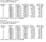
Here we are. I ran some readings on various frequencies and loads for thd and rms output.
I put that info in a spreadsheet, of which I'm attaching a screenshot here.
Those readings were all with a bias set at about 100mA per output.
I added idle power dissipation data on the schematic, so the total idle dissipation is known and should be about 20W per amp side (high & low). Since the bridge is meant to drive an 8ohms load nominally, and being able to sustain without damage a 4ohms load. There is quite a bit of power to dissipate from usage, and much more than the mere 20W from idle. So of course the heatsinks need to be big enough and they'll handle the idle easily.
I think increasing the bias can even be done safely, and it does reduce thd some more, within reason.
If the layout is such that each amp side has its own heatsink, then there is no issue with using both bias spreader transistors to sense each sink, respectively.
I think those readings are quite satisfactory, for a 3055 amp, and it seems quite stable. I have tried the square wave and it handles it well, with a slew rate around 20V/us, which is quite respectable.
The main issue with the odd behavior above a certain level having been solved by using a different type of CCS, I can drive it into clipping now.
One interesting thing to do will be to bridge this bridge again. That would be a cool thing...
Attachments
The trick to getting the grounded bridge to work right is to make sure the front end doesn't depend on a ground reference anyhwere to work right. And that both sides can tolerate sliding rails (very high PSRR and common mode range). It will work like 4 ohms loaded because it's a bridge - but because of the toploogy it is further bridgeable! That means you really want a 2 ohm capable OPS....
I was unable to get the simulation to work right once bridged. I know I'm still very far from being an ltspice expert, so there may be an issue there, but from what I gather so far, we may have something wrong with that crown divider at the low side input. This seems wrong because of a huge gain difference, from what I understand, and it makes it clip so hard that we get square wave out, with oscillations.
Someone more skilled than me needs to sim this and perhaps find what is wrong. We're so close to a working amp, we can finish this and make pcbs (protos).
With a bunch of small improvements, I was able to drop the thd a bunch and get a slew rate at something like 20V/us. More properly run sims could reveal further improvements, mostly for stability, as I think the phase margin isn't good enough.
As far as the complementary "john ellis" bridge ") is concerned, it's looking real nice now, after finding out why it behaved oddly and changing the ltp ccs type.
is concerned, it's looking real nice now, after finding out why it behaved oddly and changing the ltp ccs type.
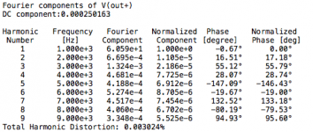
I've been running many sims and since the phase margin was very thin, I ended up adjusting cap values, C2-C3-C9-C10 are now at 4p7 and I upped the miller caps to 120p. The thd went down as a result, at 20khz at full power before clipping (some 226W on that sim) the drop is more than 40ppm, to just below 189ppm, very decent for such amp. At 1khz we're at about 30ppm. (see attached)
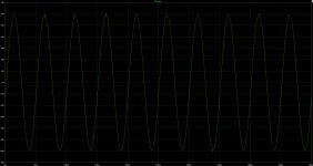
There is one thing that I am wondering about though. The phase margin is now at some 36degrees, with a bandwidth of about 389khz and a power bandwidth of about 132khz. However after running the sim with a smaller step, I now see some tiny glitches, which look like very hf oscillation (see sine wave plot attached). That is probably what accounts for most of the 189ppm of thd.
I wonder if we should address this, if it can be curbed, or just leave it as is.
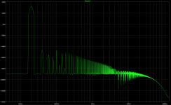
The attached FFT plot at 20khz doesn't look too shaby as well.
I ran the sims for an output of 100W at 1khz and 20khz and the thd goes down to some 161ppm for 20khz and 16ppm for 1khz.
I have some questions though:
1) shouldn't the speed-up caps C5-C8 be a little bigger? we have 1u now.
2) how can we provide the equivalent of the center tap from the psu without having a psu having one? I tried using a resistor divider, but that didn't work, I suppose because of the variations due to the changing current drawn from it, as small as that is.
3) shouldn't we be able to block DC at the input? We can't insert caps in series on both inputs, as that would prevent using it with a non balanced signal when needed. If a non balanced use is needed, I think a simple different cable that grounds the negative input could work. Although the signal strength needed would double to get the same power output.
is concerned, it's looking real nice now, after finding out why it behaved oddly and changing the ltp ccs type.I've been running many sims and since the phase margin was very thin, I ended up adjusting cap values, C2-C3-C9-C10 are now at 4p7 and I upped the miller caps to 120p. The thd went down as a result, at 20khz at full power before clipping (some 226W on that sim) the drop is more than 40ppm, to just below 189ppm, very decent for such amp. At 1khz we're at about 30ppm. (see attached)
There is one thing that I am wondering about though. The phase margin is now at some 36degrees, with a bandwidth of about 389khz and a power bandwidth of about 132khz. However after running the sim with a smaller step, I now see some tiny glitches, which look like very hf oscillation (see sine wave plot attached). That is probably what accounts for most of the 189ppm of thd.
I wonder if we should address this, if it can be curbed, or just leave it as is.
The attached FFT plot at 20khz doesn't look too shaby as well.
I ran the sims for an output of 100W at 1khz and 20khz and the thd goes down to some 161ppm for 20khz and 16ppm for 1khz.
I have some questions though:
1) shouldn't the speed-up caps C5-C8 be a little bigger? we have 1u now.
2) how can we provide the equivalent of the center tap from the psu without having a psu having one? I tried using a resistor divider, but that didn't work, I suppose because of the variations due to the changing current drawn from it, as small as that is.
3) shouldn't we be able to block DC at the input? We can't insert caps in series on both inputs, as that would prevent using it with a non balanced signal when needed. If a non balanced use is needed, I think a simple different cable that grounds the negative input could work. Although the signal strength needed would double to get the same power output.
Attachments
-
 Screen Shot 2014-02-26 at 7.24.07 PM.png36.1 KB · Views: 54
 -
 Screen Shot 2014-02-26 at 7.20.23 PM.png158.6 KB · Views: 50
 -
 Screen Shot 2014-02-26 at 7.11.37 PM.png68 KB · Views: 39
 -
 Screen Shot 2014-02-26 at 7.10.53 PM.png269.9 KB · Views: 63
 -
 Screen Shot 2014-02-26 at 8.01.41 PM.png433.9 KB · Views: 85
Here are 2 sim files with the models file used.
The high side worked fine by itself and also in those sims in the bridge if I make a split psu with the center tap at ground and I isolate the low side from it.
The low side can also work somewhat, when making slight changes, such as ungrounding its output, on a split psu of course, giving it a load and unhooking that input network and giving it a tiny sine wave to drive it. Since it doesn't have a feedback, we have an open loop on that side by itself.
I tried changing the divider network's values, but so far no luck. It always drives into very hard clipping and ends with with some modulated low amplitude square wave on the output.
Something isn't right, but I haven't found out what. Hopefully it isn't much and it can be made to work without major changes.
I was basically done with the single sided proto boards for that amp, but since the sims show it's not working right, this should be addressed before attempting making a proto. Good thing I did the sims, so we know something needs to be done. Better find this out now virtually, before making anything...
Attachments
I was experimenting with a simulation using a different output stage topo that would be more linear and have other advantages. I started from the way bryston does its output tripples, in a complementary way. but mixing the npn and pnp on each side, to compensate for the differences between them.
I made a simulation using the ordinary input ltp with ccs and mirrors, plus a vas with 2 transistors loaded by a css as well. Then after wrestling with instabilities in that sensitive output stage, it did turn out very nice. As long as the oscillations are tamed, the thd is very low, even on heavy loads and I was able to make a stable amp, fairly fast, good enough bandwidth and that was able to do fairly well on square waves with a slew rate in the 33V/us range.
Then I figured if this works well, I could slap 2N3055 on there to see how much more I could squeeze out of those babies. So this works out nicely as well, with higher thd than the mjl4281 types for example, but not bad at all, as I got down to between 10 and 20ppm at 20khz on 8ohms.
Then I thought why not applying this output stage on the elektor based amp that we've been working on. And I managed to get something rather nice as well, and much better than the best I got earlier from improvements. That amp now has a slew rate that seems higher than 40V/us, on a 4ohms load, the thd at 20k is below 30ppm. I made some compromises to keep the high slew rate, stability and keep the thd reasonably low. At first I managed the thd to drop below 17ppm, with a good stability, or so it seemed, because the square wave simulation shows something that was not happening with the mjl parts. Only the 3055s are showing this and I haven't been able to make it go away completely. Basically it's a glitch at the cross over on the very steep rise on the square waves. This distortion doesn't show up at all on any frequency sine waves, only the fast rise squares.
I'm attaching a screenshot showing this. I am wondering if someone knew how to get rid of this without trying to compensate further and cause more distortion.
Perhaps this can be tamed precisely with a properly calibrated snubber somewhere on the output stage. But how to calculate the values and where to place that optimally?
This version of the amp is complementary, so it's not the quasi we're working on now, and because of its topology on the output stage, it can't be made with an odd number of pairs. So since the amp could be subjected to 2ohm loads, instead of 2 pairs, I opted for 4 pairs. This works great actually, because the simulations on the 2ohms load at 20khz shows the thd at about 50ppm, at max power (217W).
Attachments
- Home
- Amplifiers
- Solid State
- Amplifier based on 2N3055