How are the j113/j175 noise wise ?
Hi Georg,
I have checked the noise at the oscilloscope and it is mainly 100 Hz which seems to be power supply problem and/or gnd layuot problem. Now i will rework the power supply and will tell you the result. I hope the problem will be in the power supply because the other problem may be the PCB layout which will demand a new pcb to be developed.
Can you tell me the value of the R32. I mean the input resistance at front jfets?
Best regards
...
I have checked the noise at the oscilloscope and it is mainly 100 Hz which seems to be power supply problem and/or gnd layuot problem. Now i will rework the power supply and will tell you the result. ...
I like your build which allows various Fets to be tested. There aren´t many p-channel
options left unfortunately. How about 2n5461 (Fairchild) ?
Do you have the possibilty to check distortion spectra (FFT) ? (with ARTA for example).
Can you tell me the value of the R32. I mean the input resistance at front jfets?
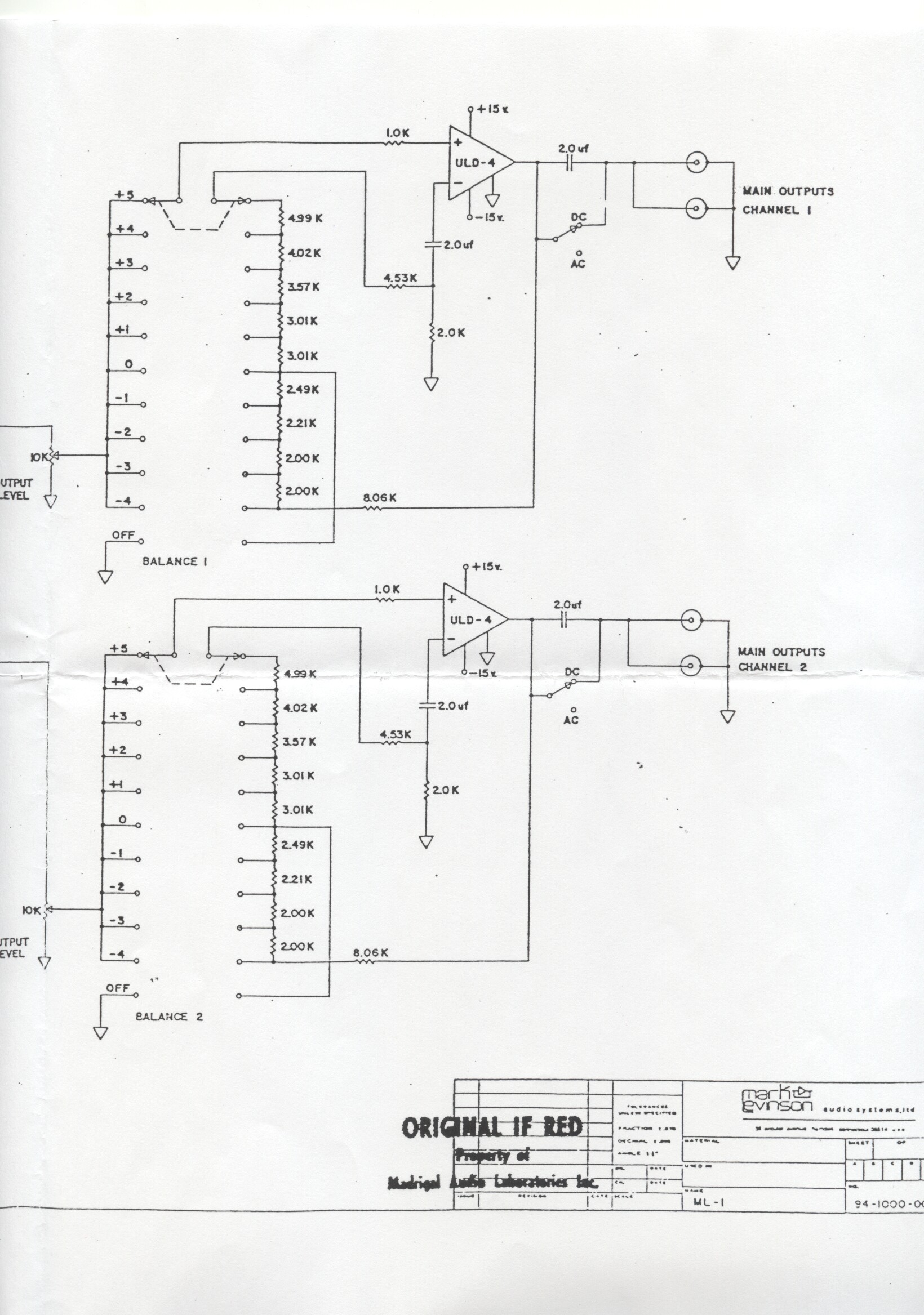
On my original ML-1 it´s 1kOhm, schematic:
http://www.diyaudio.com/forums/solid-state/10160-need-build-jc-2-preamp-8.html#post3407627
Ivo, your test is interesting. The difference between to two is that the 2sk246/j103 combination has too low of working current and too low Gm, to give adequate low Z drive to the second stage. The open loop gains 'might' be similar, but the distortion generation by the second stage will be different between the two gain modules.
Thank you Mr. Curl for your explanation,
Finally I found better matched pairs jfets j113/j175 at Idss 25.5mA. Acording to your 60% rule this will give me 15.3 mA trough jfets. With 100 Ohm load resistor this will give me about 33mA trough 2n4401/03. In that case I will have lower Z out from the first stage which is good but this will keep current in 2n4401/03 a little lower.
What happens if I go over 60% Rule? Do you know approximately the value of the input impedance of the second stage at the 30-40mA of the transistors? Is it going to be directly proportional to the peak Ft and Cbe of the output transistors? Or I miss something?
Best regars
Ivo
Hi Georg,
Look at datasheet. 2n5461 is not possible to be used here.
No. I don't have necessary equipment to make this test. I think mr. John Curl have made this test in the past.
Regards
How about 2n5461 (Fairchild) ?
Look at datasheet. 2n5461 is not possible to be used here.
Do you have the possibilty to check distortion spectra (FFT) ? (with ARTA for example).
No. I don't have necessary equipment to make this test. I think mr. John Curl have made this test in the past.
Regards
Ok, sorry haven´t looked at the 2N5461 datasheet.
For the distortion spectra: What I meant was to compare the Toshiba FETs I use
and the J113/J175 from current production. Additionally I have an original module
too. I don´t think John has made such a comparison, he designed this line stage
40 years ago and the FETs originally used are not made any more since decades.
33mA trough 2n4401/03 - that´s a lot (almost 500mW with 15V, thus near their
maximum rating at 25 deg. C). (That´s why I use TO126 style transistors in that place.)
Is it going to be directly proportional to the peak Ft and Cbe of the output transistors?
I am sorry it is my mistake, I mean directly proportional to the peak beta
sorry guys, I can't get it: J113 has a min Idss of 2mA (J112 has 5mA and J111 has 20mA), while J175 has 7ma<Idss<70mA. So, from the datasheet, they don't seem a complementary pair!
Ciao
Paolo
Look at the parameter interactions graphics from datasheets. For j113 at Vgs(off)=-2V and for j175 at Vgs(off)=4.5V. The rest will be done by the ressistor between jfets.
Look at the parameter interactions graphics from datasheets. For j113 at Vgs(off)=-2V and for j175 at Vgs(off)=4.5V. The rest will be done by the ressistor between jfets.
I was thinking that the matching (in Idss AND Vgs(off)) is important, but you are saying that the difference in Vgs(off) of a factor of 2 is good, right?
When you say that "Finally I found better matched pairs jfets j113/j175 at Idss 25.5mA", is this meaning that you have selected 2 x 4 fets (2 pieces J113 and 2 pieces J175 for each channel) that have Idss = 25.5mA? And what about Vgs(off)?
As Andrew said, the curve Id vs Vgs should be equal in order to consider them matched, and I don't understand if you matched them for Idss, Vgs(off), both or none....
Thanks for your informations,
Paolo
Paolo,
Vgs(off) is graphical curve produced by a manufacturer in order to facilitate users. because at the beginning we do not know which one part to buy (j112 or j113). What we know in the begining are that we need for example jfets with 22mA at Idss. Now we look at datasheet graphic "Transfer Characteristics" and you will see that the part wiht 22mA Idss have curve with Vgs(off)=-2V. Again at datasheet we will see that the part J113 have Vgs(off) from -0.5 to -3V or average Vgs(off) =-1.75V. For J112 average it will be Vgs(off)=-3V. Now if you buy 100 pcs. from J113 and J112 and measure them you will see that from J113 you will have more jfets with 22mA than J 112. About matching procedure please read here:
http://www.geofex.com/article_folders/fetmatch/fetmatch.htm
Regards
Ok, sorry haven´t looked at the 2N5461 datasheet.
For the distortion spectra: What I meant was to compare the Toshiba FETs I use
and the J113/J175 from current production. Additionally I have an original module
too. I don´t think John has made such a comparison, he designed this line stage
40 years ago and the FETs originally used are not made any more since decades.
Georg,
I have not 2sj74 on stock. Also I have not necessary equipment to make this test valid. If you want I will send to you perfectly matched pairs J113/j175 and 2n4401/03 to make this test and to compare the results with Toshiba FETs. And before 40 years ago and now the required jfets specification for JC2 are the same - high input impedance, low input capacitance, high gm, low noise, high current, low Rds on. Except for the noisy j175 everything seems to be ok for j113/j175. Do you have 2sk246/2sj103 on stok? Do you make test between 2sk170/2sj74 and 2sk246/2sj103? Also can you measure the power consumption of the origial line modul and output dc offset?
Regards
Georg,
If you want I will send to you perfectly matched pairs J113/j175 and 2n4401/03 to make this test and to compare the results with Toshiba FETs.
Thank you for the offer, but I don´t have line module boards left and
currently have no plans to have new ones made.
Except for the noisy j175 everything seems to be ok for j113/j175.
Well yes of course, I actually regard that as good news because they
are still available while Toshiba seems not to make any p-channel FETs
any more.
Do you have 2sk246/2sj103 on stok? Do you make test between 2sk170/2sj74 and 2sk246/2sj103?
No and no. I have built my replacement modules with quad matched 2SK170V / 2SJ74V
parts which were still available at the time:
http://www.diyaudio.com/forums/solid-state/10160-need-build-jc-2-preamp-4.html#post2092626
Also can you measure the power consumption of the origial line modul and output dc offset?
According to the photo posted here
http://www.diyaudio.com/forums/solid-state/10160-need-build-jc-2-preamp-4.html#post1768266
power consumption should be 32mA and offset of this example is 25mV.
Later versions of these modules have a potentiometer to adjust offset.
View attachment 341888
As Andrew already said the two jfets are matched if they have the same curve Id vs Vgs. My jfets are matched for Idss and Vgs.
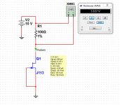
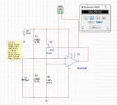
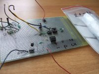
Measuring the jfets only at Idss are not very accurate because of the heat they are making. I use Idss meassuring only to put them in rough groups(see the picture1). Vgs measuring are more accurate because you can choose a lower working points that you prefer (see the picture2, R3 sets working point). The parts with equal Vgs at two working points (for example at 15mA and 5mA) will have almost identical curve. Remember that measuring should be done at constant room temperature. At picture3 you will see my Jfet matcher, it is ugly but works well.
Regards
As Andrew said, the curve Id vs Vgs should be equal in order to consider them matched, and I don't understand if you matched them for Idss, Vgs(off), both or none....
As Andrew already said the two jfets are matched if they have the same curve Id vs Vgs. My jfets are matched for Idss and Vgs.
Measuring the jfets only at Idss are not very accurate because of the heat they are making. I use Idss meassuring only to put them in rough groups(see the picture1). Vgs measuring are more accurate because you can choose a lower working points that you prefer (see the picture2, R3 sets working point). The parts with equal Vgs at two working points (for example at 15mA and 5mA) will have almost identical curve. Remember that measuring should be done at constant room temperature. At picture3 you will see my Jfet matcher, it is ugly but works well.
Regards
Attachments
I think he meant to say that the jFETS are Vgs matched at two Id set points.
Note that diag 1 is not measusing Idss. Vds is ~8.2Vds and varies with each device.
Note that diag 2 has a need for exactly repeatable 10.xyzVdc supply.
You're right of course,
The voltage drop across the resistor must be taken into account. But for roughly grouping will do the job.
Thanks for the correction
According to the photo posted here
http://www.diyaudio.com/forums/solid-state/10160-need-build-jc-2-preamp-4.html#post1768266
power consumption should be 32mA and offset of this example is 25mV.
Later versions of these modules have a potentiometer to adjust offset.
Georg,
You have original modul which is great advanage. Your line modul is with two potentiometers - right? It is important to know do you have any DC offset?
By the way the power supply problem was resolved
")
Regards
Attachments
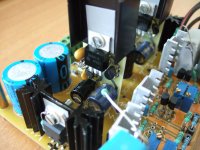
View attachment 341888
As Andrew already said the two jfets are matched if they have the same curve Id vs Vgs. My jfets are matched for Idss and Vgs.
Measuring the jfets only at Idss are not very accurate because of the heat they are making. I use Idss meassuring only to put them in rough groups(see the picture1). Vgs measuring are more accurate because you can choose a lower working points that you prefer (see the picture2, R3 sets working point). The parts with equal Vgs at two working points (for example at 15mA and 5mA) will have almost identical curve. Remember that measuring should be done at constant room temperature. At picture3 you will see my Jfet matcher, it is ugly but works well.
Regards
Thank you ivodonchev, now it is clear. I have infact noticed that the Idss measurement changes with time after the voltage switch on, due to the heating of the fet. For this reason I take the measurement just after few seconds from the start.
Ciao
Paolo
gk7, I have a question for you, if you don't mind..
This line stage schematic you've posted some time ago - transistor types aside, does it represent what was in original module or are there any additions/omissins by you?
Particulary, I'd like to know whether C1; C2; C3; C4 and R6; R7; R8; R9 were inside it.
I have a ML schematic that also shows ULD-4 module and I'd like to understand how all internal and external parts interract.
Thanks!
Attachments
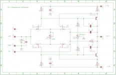
My schematic (and what I built and use, as described here in this thread) is based on
the schematic of John published. What is inside the modules I don´t know they are
potted with epoxy:
http://www.hal9000.at/audio/JC-2/ml1-project/l1000114_jpg.jpeg
R8, R9, R10 are not present in Johns schematic, but my original modules obviously have
a second pot for offset adjustment so I "borrowed" this from the ML-2 power amplifier
which uses the same topology as input stage. It works well.
R6 is only needed if you use that 2u cap in the feedback loop:
http://www.diyaudio.com/forums/atta...3101224-need-build-jc-2-preamp-ml-1_main2.jpg
it´s the feedback path for DC and certainly must be present in the original modules.
C1; C2; C3; C4 are in the original schematic.
Please post it, I´m curious to see it.
the schematic of John published. What is inside the modules I don´t know they are
potted with epoxy:
http://www.hal9000.at/audio/JC-2/ml1-project/l1000114_jpg.jpeg
R8, R9, R10 are not present in Johns schematic, but my original modules obviously have
a second pot for offset adjustment so I "borrowed" this from the ML-2 power amplifier
which uses the same topology as input stage. It works well.
R6 is only needed if you use that 2u cap in the feedback loop:
http://www.diyaudio.com/forums/atta...3101224-need-build-jc-2-preamp-ml-1_main2.jpg
it´s the feedback path for DC and certainly must be present in the original modules.
C1; C2; C3; C4 are in the original schematic.
...
I have a ML schematic that also shows ULD-4 module ...
Please post it, I´m curious to see it.
- Home
- Source & Line
- Analog Line Level
- Need to build JC 2 preamp