Hi Guys
Ed, what Self and Leech said was and is relevant to the discussion you participated in regarding parallel output devices and et al. No they did not mention class-i but then neither did you until your last post. Whereas most of my posts explicitly discussed class-i.
Andrew T, please reread.
Have fun
Kevin O'Connor
Hi Guys
Ed, what Self and Leech said was and is relevant to the discussion you participated in regarding parallel output devices and et al. No they did not mention class-i but then neither did you until your last post. Whereas most of my posts explicitly discussed class-i.
Andrew T, please reread.
Have fun
Kevin O'Connor
http://www.diyaudio.com/forums/solid-state/202684-class-i-siblings-17.html

Re #82 and prev.
This is obfuscation. You are clearly avoiding discussion of the OP but why distract those who want to continue?
The point is, that those reading this thread can expect to see discussion about class i, not just more flag-waving
for the conventional approaches, views and gurus, who already have their overwhelming share of airplay here.
Hi Guys
Ed, what Self and Leech said was and is relevant to the discussion you participated in regarding parallel output devices and et al. No they did not mention class-i but then neither did you until your last post. Whereas most of my posts explicitly discussed class-i.
Andrew T, please reread.
Have fun
Kevin O'Connor
First, my name is Edmond, while Ed is an abbreviation of Edward.
Second, >but then neither did you
Is that so? See post #8 and in particular this thread: http://www.diyaudio.com/forums/solid-state/202684-class-i-siblings.html#post2824692
And please, read this thread first before dropping any further comments.
Third, you participated in regarding parallel output devices
True. 'Some people are more equal'.
To all: To revitalize this thread I like to put a few more remarks about class-i and similar circuits (e.g. AB2):
1. The sliding bias does NOT lower the distortion. Quite the opposite: it increases the distortion by a factor two to three (at least in case of a MOSFET OPS, I don't how a BJT OPS behaves).
Why? Because the bias voltage is heavily modulated.
Why it is modulated that way? Because both legs of the OPS are never turned off completely.
And why is that? Because you can't control Iq if one of the OP devices is completely turned off. No current means no information to undertake some action.
Nevertheless, such 'non switching' amps are advertised as beneficial, which IMHO is just marketing blah blah.
The only advantage is that it copes far better with thermal transitions, as the bias voltage (and Iq) is immediately adjusted.
2. Despite above remarks, the distortion of class-i and siblings is far less then amps with a fixed (well, only temperature dependent) bias. This has nothing to do with the sliding bias. Instead, it's due to a second (differential) feedback loop, which locally provides error feedback to the OPS. As a result, the distortion increase from the sliding bias is more than outweighed by the second error correction FB loop.
Cheers,
E.
Last edited:
Edmond,
trying to follow your (1.).
are you asserting that there is no distortion reduction by keeping the output devices from switching off (class AB) there is no distortion benefit per se?
Also, are you saying that the "tracking signal" that prevents the switch off is in fact a second feedback loop that effects each side of the output stage that is conducting??
It would seem that what one would want is for example if the postive rail devices that are being driven "off" and then the signal swinging "negative" that at some theshold at nearly cutoff, that what is wanted is a voltage - essentially the inverse of the signal driving negative subtracted from the negative going signal - applied to the positive transistor. But only when it is at the cutoff threshold and below. In other words never apply an AC signal that can drive either rail into cutoff, or more precisely, apply a signal that forces the output device to just stay on.
Now, what I am completely unclear on is if this in fact is possible and if it is being done, or if some other means is being used in Class i or other "non switching" amp. And, is this a distortion canceling feedback mechanism?
Sorry to admit to being unclear on this, I'm sure some time with these circuits and a simulator would make it much more clear...
_-_-bear
>"...the nonlinear switching bias circuitry although performing its primary function may actually accentuates crossover distortion."
Thx Walter.
Edmond,
trying to follow your (1.).
are you asserting that there is no distortion reduction by keeping the output devices from switching off (class AB) there is no distortion benefit per se?
Hi Bear,
Yes, that's correct.
Also, are you saying that the "tracking signal" that prevents the switch off is in fact a second feedback loop that effects each side of the output stage that is conducting??
Yes. There are two FB loops: one differential loop that provides local error feedback and one common mode loop that controles the bias. It's the latter loop that may increase distortion (in case of class-i and also my AB2 circuit, for example).
It would seem that what one would want is for example if the postive rail devices that are being driven "off" and then the signal swinging "negative" that at some theshold at nearly cutoff, that what is wanted is a voltage - essentially the inverse of the signal driving negative subtracted from the negative going signal - applied to the positive transistor. But only when it is at the cutoff threshold and below. In other words never apply an AC signal that can drive either rail into cutoff, or more precisely, apply a signal that forces the output device to just stay on.
Now, what I am completely unclear on is if this in fact is possible and if it is being done, or if some other means is being used in Class i or other "non switching" amp. And, is this a distortion canceling feedback mechanism?
Sorry to admit to being unclear on this, I'm sure some time with these circuits and a simulator would make it much more clear...
_-_-bear
To understand how class-i works, it helps to realize that that are two FB loops, as already mentioned above. As for the 2nd loop (bias control), your description above is correct. BUT... -quite unexpectedly!- the harmonic content of the difference between input and output voltage (of the OPS) is larger compared to a configuration with a fixed bias. At first instance I also didn't believe my eyes when I simulated these circuits. Yet it's true and confirmed by M.H.
BTW, I'm only talking about MOSFETs. As for BJTs the picture gets even more complicated because of the storage effect of the majority carriers, which also come into play.
Cheer,
E.
There are exceptions: I can think of at least two, the Renardson scheme, and the Circlophone.>"...the nonlinear switching bias circuitry although performing its primary function may actually accentuates crossover distortion."
Thx Walter.
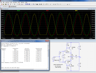
In the Circlophone, the servo circuit participates to the global linearization of the amplifier.
This is easily seen by disabling the servo, and replacing it by a fixed bias of identical average value:
Attachments
At first instance I also didn't believe my eyes when I simulated these circuits.
You don't have to believe your eyes, but to use your brain. It is obvious why crossover distortion increases, if you give up the popular misconception that output devices "switching" is mostly responsible for crosover distortion. In fact, it is gm doubling around the crossover largely responsible for the "crossover distortion". More overlapping -> more non-linear total transconductance -> more distortion.
http://users.ece.gatech.edu/mleach/papers/classab.pdf
Heavy bias towards class A and the transconductance hump flattens away, to the point to which the gm doubling effect is negligible compared to other distortion mechanisms.
Heavy bias towards class A and the transconductance hump flattens away, to the point to which the gm doubling effect is negligible compared to other distortion mechanisms.
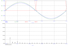
Not really: heavier bias results in heavier distortion, see example below which is the continuation of those:
http://www.diyaudio.com/forums/solid-state/222133-class-i-5.html#post3282877
Of course, if the signal is low enough to stay mainly in the class A region, the THD will begin to decrease.
The worst case, independent of the absolute level of bias, is when the signal is processed half class A and half class B.
Attachments
Of course, if the signal is low enough to stay mainly in the class A region, the THD will begin to decrease.
This is what I am talking about, not closely above the Oliver bias point.
gm doubling?
I suppose that's not meant to be derogatory.
As far as my concerns, I'm not suffering from that misconception.
In this particular case, I don't think gm doubling is the culprit. It is the modulation of the bias voltage that is responsible for the increase of THD.
Also my sims didn't reveal gm doubling.
You don't have to believe your eyes, but to use your brain.
I suppose that's not meant to be derogatory.
It is obvious why crossover distortion increases, if you give up the popular misconception that output devices "switching" is mostly responsible for crosover distortion.
As far as my concerns, I'm not suffering from that misconception.
In fact, it is gm doubling around the crossover largely responsible for the "crossover distortion". More overlapping -> more non-linear total transconductance -> more distortion.
http://users.ece.gatech.edu/mleach/papers/classab.pdf
Heavy bias towards class A and the transconductance hump flattens away, to the point to which the gm doubling effect is negligible compared to other distortion mechanisms.
In this particular case, I don't think gm doubling is the culprit. It is the modulation of the bias voltage that is responsible for the increase of THD.
Also my sims didn't reveal gm doubling.
some amplifiers are quite nervous in the way they portray the events..others have a more stable way of presenting things, more focus.. Like a clearer portrait of the music going on. Like better separation of the sound from the bow, string and body of the violin yet all emerging from the same instrument at the same position. Better focus.
Ever tried a Leica with a summicron lens..??
Ever tried a Leica with a summicron lens..??
Hang on...
Increasing the bias, up via "high bias AB" moves the transition between two rails of devices (in case we're talking multiple devices in parallel) to only one rail at a power higher in level... it has been said that this creates *more* distortion than the low level "crossover distortion" (gm doubling or not).
And is the pervasive thinking that gm doubling *is* (or gm halving, depending on which way you look at it) or is *not* the explanation for why there is crossover distortion or not?
The other issue that seems undocumented and not discussed is what the spectra of distortion for these several variations (M.H.'s for example, etc...) actually looks like. Clearly the absolute level may be of less interest than the distribution of distortion, and of course the effect on distortion as power and frequency both or independently rise. Wondering if this has been looked at?
Hi bear,..........
It would seem that what one would want is for example if the postive rail devices that are being driven "off" and then the signal swinging "negative" that at some theshold at nearly cutoff, that what is wanted is a voltage - essentially the inverse of the signal driving negative subtracted from the negative going signal - applied to the positive transistor. But only when it is at the cutoff threshold and below. In other words never apply an AC signal that can drive either rail into cutoff, or more precisely, apply a signal that forces the output device to just stay on.
.....
_-_-bear
Indeed, that's one of the things class-i does (by means of the 2nd common mode control loop).
What I'm saying is that it is this mechanism that contributes to more distortion (the distortion diminishing effect of the other loop is another story).
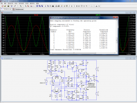
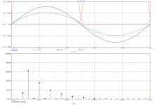
I hope it helps when I visualize the effect of common mode control loop. So let's look at the difference between input and output voltage of the OPS (i.e. the residual). Notice that the input voltage is defined as the mean value of the base (or gate) voltage of the 'top' respectively 'bottom' OP device (i.e. (Vb-npn + Vb-pnp)/2 ). This makes sense as in a typical amp with sliding bias, Cdom is split into two halves, one connected to the (input of the) top driver and the other connected to the bottom driver (see: Bob Cordell about the LT1166).
Fig. 1 depicts the behavior of an OPS with fixed bias.
Blue = output voltage,
Red = emitter currents
Green = residual
Black = harmonics.
The residual looks almost like a perfect sine and indeed, the distortion is quite low: 0.03%.; mainly 2nd harmonic distortion due to non-ideal complementarity of the OP devices.
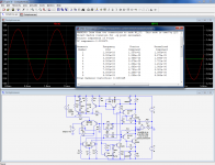
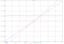
Fig. 2 depicts the behavior of an OPS with a sliding bias.
As expected, the amplitude of the residual is smaller. Simply because the OP devices are never turned off completely. BUT.... the shape of this residual is far more distorted. As a result, THD is about 2.5 time higher, mainly 3rd harmonics.
BTW, this has nothing to with gm doubling inside the crossover region, rather an increase of gm far outside the crossover region.
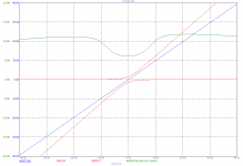
See fig.3: gm with fixed bias and Fig. 4: gm with sliding bias (green curves).
Cheers,
E.
Attachments
- Status
- This old topic is closed. If you want to reopen this topic, contact a moderator using the "Report Post" button.
- Home
- Amplifiers
- Solid State
- Class i