How much DC current can be allowed on the transformer primary without detectably increasing distortion? I am trying to avoid yet another capacitor between the JFET follower driver and the transformer primary. The the JFET source resistor(s) can be trimmed to zero the follower output voltage, but during output FET bias adjustment the output voltage divided by the closed-loop gain could easily be 20mV or more. That would be about 1mA in each primary winding.
....... but during output FET bias adjustment the output voltage divided by the closed-loop gain could easily be 20mV or more........
no harm from that
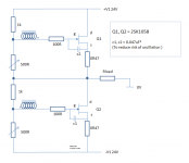
Fired up the iron again... I tried the simple resistor bias network again and it seems to work quite ok. No global feedback and i haven't yet done the front end buffer.
Schematic attached in case someone wants to have a bash - I did not make any effort to match fets.
With these Hitachi lateral parts, there seems to be a tendency toward oscillation when two same polarity fets are nearby (I didn’t see this when I was using complementaries) - I 'cured' this with two small caps - and saw later that Hiraga did the same in the nemesis so perhaps I am not alone here.
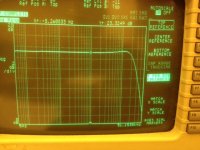
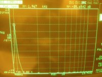
Freq response is 5Hz-20Khz -0.5db so that's ok i think - I did not try loading the TX. The fets were biased up to 1.4A so that works out to be about 25W rms in class A. 1 Watt is very clean @ 0.02%, 10W 0.07%, 20W 0.15%, 30W 0.2%, 60W 0.5% and it hits close to 1% at 80W.
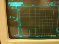
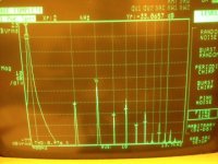
1W, 20W, 50W and 80W clipping spectra attached - looks fairly ok to me (take a look at Paul Millers measurement QC Suite results website for some popular amps to see some comparisons at clipping).
I had to truncate the spectra at a bit over H13 (there was nothing I could see further out) because I was getting some interference from the room lights that I couldn’t fix.
Total gain incl i/p stepup tx is 14x (23db.)
Next steps: try the R100s when they arrive (thanks TB!), build the front end jfet buffers and listening tests.
Schematic attached in case someone wants to have a bash - I did not make any effort to match fets.
With these Hitachi lateral parts, there seems to be a tendency toward oscillation when two same polarity fets are nearby (I didn’t see this when I was using complementaries) - I 'cured' this with two small caps - and saw later that Hiraga did the same in the nemesis so perhaps I am not alone here.
Freq response is 5Hz-20Khz -0.5db so that's ok i think - I did not try loading the TX. The fets were biased up to 1.4A so that works out to be about 25W rms in class A. 1 Watt is very clean @ 0.02%, 10W 0.07%, 20W 0.15%, 30W 0.2%, 60W 0.5% and it hits close to 1% at 80W.
1W, 20W, 50W and 80W clipping spectra attached - looks fairly ok to me (take a look at Paul Millers measurement QC Suite results website for some popular amps to see some comparisons at clipping).
I had to truncate the spectra at a bit over H13 (there was nothing I could see further out) because I was getting some interference from the room lights that I couldn’t fix.
Total gain incl i/p stepup tx is 14x (23db.)
Next steps: try the R100s when they arrive (thanks TB!), build the front end jfet buffers and listening tests.
Attachments
Last edited:
kasey,
Where is your circuit. I have the laterals and would like to give it a whirl. Don't have enough to do.
haha - sorry missed it - just attached....
you have Dc bias going through coil? hasn't ZM been trying to avoid that. Perhaps you have heftier transformer, as do I.
I didn't think that the bias current was material - as its just the miniscule GS leakage current. Perhaps, as you point out, it may be relevant with the smaller linestage transformers but not for the power trannies I used. Have a bash and see what you find ....
With enough monkeys on typewriters for long enough we will design all of the future works of Nelson Pass.
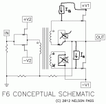
Here is another F6 bias circuit design using zener diodes instead of batteries or voltage regulators. The component count is somewhat smaller, and it simulates well.
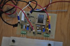
The photo is my prototype for the schematic in post 729 http://www.diyaudio.com/forums/pass-labs/216616-f6-amplifier-73.html#post3123858. I need some tweaks for the bias generators since I used red LEDs instead of zeners and the voltage is a bit to low to get 1.3A bias with .12 ohm source resistors. Lots of testing still to be done.
Note the NP (Nelson Pass) label on the capacitors.

Attachments
The photo is my prototype for the schematic in post 729 http://www.diyaudio.com/forums/pass-labs/216616-f6-amplifier-73.html#post3123858. I need some tweaks for the bias generators since I used red LEDs instead of zeners and the voltage is a bit to low to get 1.3A bias with .12 ohm source resistors. Lots of testing still to be done.
Note the NP (Nelson Pass) label on the capacitors.
nice
share some results when you get a chance ....kasey197, you wrote: Next steps: try the R100s when they arrive (thanks TB!), build the front end jfet buffers and listening tests.
You are a patient person. If I was in your shoes, I would have already connected the primary of the Jensen transformer to an R or L headphone output channel [which is volume controlled] of a CD player. Listen to your creation as you go along. Once you put together the front end and integrate the amplifier, my proposed listening experiment will never ever entertain your ears! Best regards.
You are a patient person. If I was in your shoes, I would have already connected the primary of the Jensen transformer to an R or L headphone output channel [which is volume controlled] of a CD player. Listen to your creation as you go along. Once you put together the front end and integrate the amplifier, my proposed listening experiment will never ever entertain your ears! Best regards.
Antoinel: Thanks and yes you're right - I'm not that patient and had it hooked it up already )
Sounds pretty nice but then mono often does to me proper listening & impressions to come in time.
In a different life, I used to review audio gear for a living ... so some (likely too little!) critical faculties still exist I feel... btw, my R100's just arrived today ... yessss!!!
)Sounds pretty nice but then mono often does to me
proper listening & impressions to come in time.In a different life, I used to review audio gear for a living ... so some (likely too little!) critical faculties still exist I feel... btw, my R100's just arrived today ... yessss!!!
Hi,
to avoid capacitors in signal path - that should be possible to use two identical DC current sources.
Drop voltage on each of secondary winding ( Resistance part ) will serve as necessary bias, and final magnetic flux remain 0.
Hopefully Mr.Pass will forgive me that "reuse" of his drawing.
to avoid capacitors in signal path - that should be possible to use two identical DC current sources.
Drop voltage on each of secondary winding ( Resistance part ) will serve as necessary bias, and final magnetic flux remain 0.
Hopefully Mr.Pass will forgive me that "reuse" of his drawing.
Attachments
F6 Design Tradeoffs
Here are some overall design tradeoffs for the F6, with the following assumptions:
Rs (Output FET source degeneration resistance):
My prototype build assumes one FET per rail and CLG=6. Tomorrow intend to start tests with Rs=.47, .24, and .12 ohms.
Here are some overall design tradeoffs for the F6, with the following assumptions:
- Post 1 http://www.diyaudio.com/forums/pass-labs/216616-f6-amplifier.html#post3100799 defines the basic design with the correction of the phase of the bottom secondary.
- No voltage gain in the transformer. Assume Jensen Transformer JT-123-FLPCH.
- All voltage gain comes from the output FETs, whose number is unspecified.
- Close loop gain is unspecified, but is expected to be between 3 and 6 or so.
- KISS (keep it simple stupid) dictates no use of (complex) servos to maintain bias.
Rs (Output FET source degeneration resistance):
- Smaller increases open-loop gain and amount of negative feedback which decreases THD.
- Larger improves bias stability.
- Larger reduces signal input voltage requirements.
- Smaller increases open-loop gain and amount of negative feedback which decreases THD.
- More increases open-loop gain and amount of negative feedback which decreases THD, but increases the need for FET Vgs matching.
- One FET per rail eliminates the need for Vgs matching.
- Semisouth R100 JFETs give high transconductance and low input capacitance.
- FQA28N15 MOSFETs have high transconductance (and are inexpensive) but have much higher input capacitance.
My prototype build assumes one FET per rail and CLG=6. Tomorrow intend to start tests with Rs=.47, .24, and .12 ohms.
Interesting idea. At 1.3A bias current thru the R100 output FETS, I see a Vgs of about 1.2V. The JT-123-FLPCH windings have a DC resistance of 28 ohms. That gives about 43mA current thru the winding, and about 1 Watt power dissipation in each bias current source assuming 25V rails. Sounds doable.Hi,
to avoid capacitors in signal path - that should be possible to use two identical DC current sources.
Drop voltage on each of secondary winding ( Resistance part ) will serve as necessary bias, and final magnetic flux remain 0.
Hopefully Mr.Pass will forgive me that "reuse" of his drawing.
lhquam, fwiw, just my thoughts... maybe try one set output fets, Rs=0.47 Ohm, feedback resistor network = 100 Ohm from output (Rf), 10ohm from tx pri to ground(Ri). Appears low I agree and perhaps the Jensens may be happy with the same ratio scaled up 5-10x ie Rf=1k, Ri = 100 ohms. No Jensens here so can't try
I do not think that the closed-loop gain should be increased beyond about 6 because of the loss of negative feedback.lhquam, fwiw, just my thoughts... maybe try one set output fets, Rs=0.47 Ohm, feedback resistor network = 100 Ohm from output (Rf), 10ohm from tx pri to ground(Ri). Appears low I agree and perhaps the Jensens may be happy with the same ratio scaled up 5-10x ie Rf=1k, Ri = 100 ohms. No Jensens here so can't try
db(feedback) = db(open-loop-gain) - db(closed-loop-gain)
My Spice simulations with one output FET per rail show the following open-loop gains (OLG), as a function of FET source resistance (Rs).
Rs .01 .1 .22 .47
OLG 99 59 39 23
With Rs=.47 and CLG=10, there is only a 2.3:1 feedback factor, unless then number of output FETS is increased.
Because of bias stability issues, I expect Rs to be greater than .1. To achieve sufficient OLG, Rs needs to be small, or the number of output FETS must be increased.
The main effect of increasing both feedback resistors by the same factor seems to be high frequency rolloff, due to the capacitance of the output FETS. At this point, I have no idea about the "optimal" value for the feedback resistors.
Last edited:
When?
Don't take this too hard, but when is the real article coming out?
I think it's great you are reverse engineering the design and more power to you. I'm just thinking all this conjecture and speculation might be holding up the real article from coming out for one reason or another.
Think about it for a second. If it's as simple as shown in your recent schematics, why hasn't the article been released yet? Maybe the explaination is bigger than anyone thinks.
Again, I respect your enthusiasm and ability. Don't take this the wrong way.
I'm just looking forward to the real article, especially if it's as simple as you are painting it to be. When I say simple I mean low parts count.
Vince
The underlined is The Pass Doctrine at work!Don't take this too hard, but when is the real article coming out?
I think it's great you are reverse engineering the design and more power I'm just looking forward to the real article, especially if it's as simple as you are painting it to be. When I say simple I mean low parts count.
Vince
- Home
- Amplifiers
- Pass Labs
- F6 Amplifier