Does anyone understand the gate to source current of SIC FETs such as the SJEP120R100 under bias conditions expected in the F6? I have never worked with these beasts before and do not know what to expect.
FET gate currents only occur under AC conditions.
Jer
")
I see them as exactly the same. Magic will be in how he manipulates them into being different.Please go to post #292. It shows the updated and simplified F6 schematic. In it, Mr. Pass readjusted the phase relationships of the secondary windings of the transformer. Go ahead and put a circle [for phase] at the output node. The phase of the signal at the output node is the same as the phase of the input signal at the upper secondary winding, and the same as the phase of the signal shown for the primary winding. I am confident that no one will challenge [you or me] that this is the correct phase and/or answer. At this point a "Eureka" light lit up my brain [and hopefully yours too]. The instantaneous and individual contribution of voltage at/to the output from the upper and the lower JFEts must always be in-phase [as declared above].
So, this is what I see as I look at the simplified F6 schematic. The upper JFET is a non-phase inverting voltage source amplifier [VSA]. It is connected in series with the bottom JFET which is a phase-inverting transconconductance amplifier [TCA]. These two amplifiers are independently controlled by the secondary windings; but they work together, and their individual contribution [of voltage and current to the load is [and must be] always in phase, and thus is additive rather than destructive.
Clearly, in good time, Mr. Pass will have the only and best explanation for the operation of his F6 creation.
I see them as exactly the same. Magic will be in how he manipulates them into being different.
The magic is they are [operating] exactly the same. In an ideal world:
- The secondary windings of transformer are identical.
- The JFETs are highly matched. Same transconductance gm = Io/Vi
- The input signals to JFETs are identical in amplitude and exactly 180 degrees out of phase.
- The source and drain currents of the upper JFET are identical.
- The source and drain currents of the lower JFET are also identical.
- Since the JFETs are highly matched, the static and dynamic drain current of the bottom JFET is equal to the source current of the upper JFET.
- The instantaneous voltage output contribution emanating from the upper JFET is identical in amplitude and phase to that emanating from the lower JFET. Neither JFET wastes current in the other by a mismatch in signal phase and/or its amplitude. Their sole focus is driving the load.
FET gate currents only occur under AC conditions.
Jer
SIC JFETs are somewhat different from MOSFETs. There is actually a PN junction between gate and source, which conducts as Vgs increases about its threshold voltage.
Minutes ago I performed a measurement of a R100A SIC FET.
Vds=14V, Idrain=1.3A, Vgs=1.17V
The gate current was 1.9uA.
Not a lot, but not zero. Not enough to worry about for transformer DC current.
Ilquam,
Wrenchone has a thread entitled " Le Fake", i believ,e where he and Nelson discuss the leakage current of the SiC parts. Perhaps you can find what you are looking for there.
I found this post by Papa which discusses gate leakage: http://www.diyaudio.com/forums/solid-state/148959-semisouth-sic-power-jfets-9.html#post2665080
SIC JFETs are somewhat different from MOSFETs. There is actually a PN junction between gate and source, which conducts as Vgs increases about its threshold voltage.
Minutes ago I performed a measurement of a R100A SIC FET.
Vds=14V, Idrain=1.3A, Vgs=1.17V
The gate current was 1.9uA.
Not a lot, but not zero. Not enough to worry about for transformer DC current.
I knew I would get some feedback about my statement and should have rephrased it.
1.9ua is not an significant amount of current compared to the current that flows during AC signal.
For give me if I have confused you.
jer
ZM pointed out in the schematic posted by Nelson, that were separate rails for FE and output stage. What does this offer us in terms of amplifier performance as well as scaling?
The transformer is essentially isolating the two from each other, with only the feedback loop acting as a connection.
The transformer is essentially isolating the two from each other, with only the feedback loop acting as a connection.
I would use a lower voltage for the FE to reduce power dissipation in the input source follower JFETs. I cannot think of any other reason, other than perhaps reducing power supply ripple.ZM pointed out in the schematic posted by Nelson, that were separate rails for FE and output stage. What does this offer us in terms of amplifier performance as well as scaling?
The transformer is essentially isolating the two from each other, with only the feedback loop acting as a connection.

....
EDit MV? megavolts?
why not ?
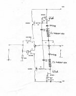
see ; +/-20V arbitrary - written for then actual chat
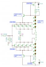
later I saw interesting idea too - called Hawksford buffer (second pic )
plain one is cascode voltage biass referenced to gnd , H. same referenced to sources - having as result that jfets are working in real constant voltage mode
search to read what's difference - lower output impedance , if I remember that well
didn't measured , didn't tried
Attachments
Last edited:
found it ...... partially - JG : http://www.diyaudio.com/forums/pass-labs/161411-buffer-preamp-shunt-ps-4.html#post2558131
Yes, i designed it. It is a driven cascode but "the other way around". Hawksford´s original
circuit had a driven cascode in the second stage. There is a paper on his website about it.
Later i heard that Borbely did the same 7 years before and that it was known to designers of Oszilloscopes.
People that build it responded that the bass was sounding better compared to the ground referenced version. It should improve distortion into low impedances.
Here we go :http://www.essex.ac.uk/csee/research/audio_lab/malcolmspubdocs/J10 Enhanced cascode.pdf
It has to do with returning or using the base current in BJT circuits that is normally lost.
I think our Dimitry made an AES paper with more details and optimization.
It has to do with returning or using the base current in BJT circuits that is normally lost.
I think our Dimitry made an AES paper with more details and optimization.
but "the other way around".
Very smart.
- Home
- Amplifiers
- Pass Labs
- F6 Amplifier