How big of a heat sink do these devices need. Do Q3, 4, 5 and 6 need to be sinked? And as for the MOSFETS, if I were to use IRF540 and IRF9540 as suggested earlier in the thread, is there a calculation to work out the heat sink size. I am used to building chip-amps, where there is a nice Excel spreadsheet to help you work out heat sink sizes.
Thanks again for all the advice")
Thanks again for all the advice
Sorry to keep asking questions, but her goes....
I understand the principle of Class D amps now, but the output of the comparator will always be a a PWM square wave. It switches N and P MOSFETS when either positive or negative right? If the output of the comparator has to be positive or negative, that means 1 of the MOSFETS (in half bridge) or 2 (full bridge) would be on all the time? If there is no input at the front end of the amp, what is happening at the speaker?
I understand the principle of Class D amps now, but the output of the comparator will always be a a PWM square wave. It switches N and P MOSFETS when either positive or negative right? If the output of the comparator has to be positive or negative, that means 1 of the MOSFETS (in half bridge) or 2 (full bridge) would be on all the time? If there is no input at the front end of the amp, what is happening at the speaker?
With zero input, the mark-space (here read up-down) ratio of the output devices is 50%. Half the time +ve, half the time -ve. Goes through the low-pass filter, averages to zero.Sorry to keep asking questions, but her goes....
I understand the principle of Class D amps now, but the output of the comparator will always be a a PWM square wave. It switches N and P MOSFETS when either positive or negative right? If the output of the comparator has to be positive or negative, that means 1 of the MOSFETS (in half bridge) or 2 (full bridge) would be on all the time? If there is no input at the front end of the amp, what is happening at the speaker?
Oh, I see. So if you PWM was say 200Khz, you have a 200Khz square wave at 50% duty and the low pass filter will not pass this so the speaker sees nothing. So even with no input signal, the MOSFETS are switching 1000s of times a second, but because of the filter, they are not passing any current, therefore not getting warm? Have I got that right?
Oh, just having another look at the circuit. Where is the actual filter?
Oh, just having another look at the circuit. Where is the actual filter?
Last edited:
Yes, though of course there are losses due to switching times, the output driving stray capacitance and such (keeping the outputs shielded should help reduce radiated RF interference). It also helps a whole lot to make sure each MOSFET turns OFF before the other one turns on.Oh, I see. So if you PWM was say 200Khz, you have a 200Khz square wave at 50% duty and the low pass filter will not pass this so the speaker sees nothing. So even with no input signal, the MOSFETS are switching 1000s of times a second, but because of the filter, they are not passing any current, therefore not getting warm? Have I got that right?
That's a good question. A speaker's voice coil itself is inductive at sufficiently high frequencies and will pass less current, but still, my guess is the voice coil will get excessively warm. I hope whoever makes this has fire insurance.Oh, just having another look at the circuit. Where is the actual filter?
Oh, there's this from earlier in the thread (bolding mone):
Interesting thread. Just to let others see something of the schematics and pcb layout more easily, here are screenshots of them. For the original pdf file, see early part of thread.
Note that the output inductor is NOT shown either on the schematic or the pcb layout - whether air or ferrite cored it probably deserves to be tied down somehow.
View attachment 276326
View attachment 276327
View attachment 276328
Cheers benb. The output part of this amp looks similar to most of the other half wave Class D amps I have seen, apart from the drawing not showing the inductor. The only problem I can see here is the dead time, there is no way of setting it, so you run into a problem of both MOSFETs being on at the same time for a very small amount of time!
benb, have you much experience with Class D amps, and if so, is this a good one to start with, or am I better off building one that uses specific ICs to drive the MOSFETs? If the later option is better, could you point me in the right direction to a simple class D schematic, preferably not using SMT ICs. Thanks again
benb, have you much experience with Class D amps, and if so, is this a good one to start with, or am I better off building one that uses specific ICs to drive the MOSFETs? If the later option is better, could you point me in the right direction to a simple class D schematic, preferably not using SMT ICs. Thanks again
I have no actual experience with Class D for audio, I just know the theory. I've used Class D to drive small motors, which is much less demanding than (good) audio.
I've had good experience doing SMT, and my suggestion is don't be too afraid to try it. Get a good magnifier, a good small-tipped iron, keep everything clean and go for it. Googling for SMT tutorial brings up this:
Surface Mount Soldering 101 Video
I've had good experience doing SMT, and my suggestion is don't be too afraid to try it. Get a good magnifier, a good small-tipped iron, keep everything clean and go for it. Googling for SMT tutorial brings up this:
Surface Mount Soldering 101 Video
Interesting thread. Just to let others see something of the schematics and pcb layout more easily, here are screenshots of them. For the original pdf file, see early part of thread.
Note that the output inductor is NOT shown either on the schematic or the pcb layout - whether air or ferrite cored it probably deserves to be tied down somehow.
View attachment 276326
View attachment 276327
View attachment 276328
Hi All, especially Simon B
I am interested in this amplifier, because the circuit is simple (and also cheap to
). I am interested to make this amp as my first class D amp. I just want to ask is, what is the components value with a DNP marking?Thanks
Last edited:
Hi!
If I understood it correctly DNP component is being utilized (used) for experimentation purposes only, they are not meant to be included in the whole circuit.
Cheers!
thanks for the reply, it answered my doubts.
Has anybody measured its frequency response and other parameters?
This is the frequency response of the simulation results. I use simetrix and tina-ti, but the result is different I don't know why?
Attachments
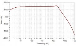
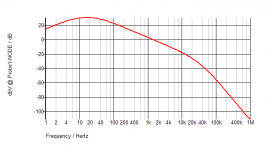
This is the frequency response of the simulation results. I use simetrix and tina-ti, but the result is different I don't know why?
This link might help you. follow the link and answers by Pafi.http://www.diyaudio.com/forums/class-d/102125-cheap-simple-class-d-amp-circuit-build-7.html#post2407027
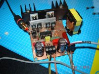
my project 2nd version
hi guys after reading through this post and ultra simple class d i have changed my layout to use bd 1xx transistors instead of 2n 5xxx . so as to make it work normal and reduce heat of output fets . i had made three circuits all i used +/-36vlts and all were heating the out put fets until i added 680r in series with 220r (r9 and r20).
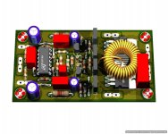
but after hearing the clarity of this amplifier i decided to use the original version which has been simulated by norazmi . here is my layout and artwork .
hi guys after reading through this post and ultra simple class d i have changed my layout to use bd 1xx transistors instead of 2n 5xxx . so as to make it work normal and reduce heat of output fets . i had made three circuits all i used +/-36vlts and all were heating the out put fets until i added 680r in series with 220r (r9 and r20).
but after hearing the clarity of this amplifier i decided to use the original version which has been simulated by norazmi . here is my layout and artwork .
Attachments
-
Class D 200 Wrms with 2 mosfet schematic .pdf26.2 KB · Views: 1,779
-
Class D 200 Wrms with 2 mosfet .zip228.4 KB · Views: 900
-
Class D 200 Wrms with 2 mosfet pcb artwork.zip831.5 KB · Views: 954
-
Class D 200 Wrms with 2 mosfet pcb top.pdf27.4 KB · Views: 881
-
Class D 200 Wrms with 2 mosfet pcb bottom.pdf22.8 KB · Views: 875
-
Class D 200 Wrms with 2 mosfet pcb components full .pdf25 KB · Views: 1,048
-
 Class D 200 Wrms with 2 mosfet -Optimized.jpg103.8 KB · Views: 2,050


- Home
- Amplifiers
- Class D
- Ultra Simple Class D