When used under sensible conditions, (i.e., ΔVin-out reasonable), 1/4W resistors are sufficient, 500mW (or 1W3 at most) zeners suffice, and the BD139 requires no more than a small cooling clip, and up to 75W output, nothing at all.What about resistor power dissipations? Has it required a heatsink for BD139 and BC337?
The BC327 needs no heatsink.
An afterthought: if you're prepared to jettison the protection completely, you can improve the performances, particularly when operated in "degraded" (electronic filter only) mode.What happens if input voltage is lower than the zener?
Thanks!
Life is a succession of hard choices.
Both are correct: the first is suitable for zener level shifting, and the second for a cascode configuration.which are the correct connection of R18 and C12
So, on selecting some devices that can literally weather a storm, the following are questions of suitability:[40v?]Yes, any zener or combination of zeners giving that voltage is suitable: 39V if 1V is not a problem, or two 20V, or 18V+22V, etc.
Q3? BC639/BCP56, 2SD669, 2N3501? a similar selection to the amplifier's phase inverter? What percentage of input voltage is seen by Q3?
Q2 surge voltage tolerance options? 2SD669, MJE344, 2SC3421, 2SC5171? Q2 sees full voltage, doesn't it?
Q1 sturdy options that may withstand a surge?
mjl21193 (16a, hfe25~75, 4mhz, 200w)
mj15004 (20a, hfe20~140, 2mhz, 250w)
mj15023 (16a, hfe15~60, 5mhz, 250w)
I tried to narrow down possible options, but I'm not knowledgeable enough to narrow it down further. We do get some huge power surges and an MOV on transformer primary doesn't seem like a complete solution.
Which resistors need to be more sturdy to withstand power surge conditions?
Approximately how much capacitance smoothing should be provided directly at each rectifier?
P.S.
It seems no problem to provide 2.5v more input than zener, because most unregulated power supplies have a sort of weak peak, charged up on noise (diode, static, line noise) of insufficient current that wasn't going to be useful to power the amp at high output levels anyway. And there is also the matter of transformer pulldown. With 2.5v margin (and 300va transformer), full output doesn't have any more than 0.2v margin remaining. Should it have more margin at full output?
Last edited:
No, it's a completely different function. Vceo>1.5V and Ic max>200mA is enough.So, on selecting some devices that can literally weather a storm, the following are questions of suitability:
Q3? BC639/BCP56, 2SD669, 2N3501? a similar selection to the amplifier's phase inverter? What percentage of input voltage is seen by Q3?
During normal operation, Q1 and Q2 see the in-out difference.Q2 surge voltage tolerance options? 2SD669, MJE344, 2SC3421, 2SC5171? Q2 sees full voltage, doesn't it?
When the protection is active, they can see up to the full input voltage, if the output is shorted.
R5 and R6 can be upgraded to 1/2WWhich resistors need to be more sturdy to withstand power surge conditions?
Something like 4700µ per 50W output is sufficientApproximately how much capacitance smoothing should be provided directly at each rectifier?
What do you mean exactly?And there is also the matter of transformer pulldown. With 2.5v margin (and 300va transformer), full output doesn't have any more than 0.2v margin remaining. Should it have more margin at full output?
CFP on the PCB..
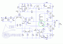
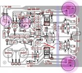
I modified powerflux's (lost?) pcb respecting CFP implementation as much as I can do. I built and tested its an earlier version with BD249C output transistors without any observable (eye for smoke,, ear for sound, fingers for heat) problem. This layout hasn't built yet.
I want to share printable pdf's after some reviews and suggestions.
Thanks.
Attachments
Last edited:
That looks fine, and anyway, since it is signal-level circuitry, the order and placement of components matters very little, and you can choose freely the most convenient configuration.I modified powerflux's (lost?) pcb respecting CFP implementation as much as I can do. I built and tested its an earlier version with BD249C output transistors without any observable (eye for smoke,, ear for sound, fingers for heat) problem. This layout hasn't built yet.
I want to share printable pdf's after some reviews and suggestions.
Thanks.
I do not know how much margin is required by the regulator board itself. A way to see the real question is: What is the minimum margin if not considering any other conditions? For example, what is the minimum margin for the regulator if fed by a source that would not have any significant rail sag?What do you mean exactly?
P.S.
I can then add to the minimum, 1v estimated rectifier noise, and also add the pull down figure from my transformer's datasheet to total up a reasonable heavy load figure to use for the difference between input voltage versus zener?
It seems ready for prospective builders..
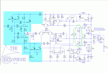
Ok, I think it is at finish for now. Amplifier itself with this layout hasn't noise pick up issue (at least with a clean source or nothing connected as source) despite its tremendous input gain.
Hope you enjoy the silence of Circlophone..
_____________________________________
 This pcb layout has reported as faulty by its author. Please refer to post #780
♫♪ My little cheap Circlophone© ♫♪
Follow later posts for fixed and actual version.
_____________________________________
Ok, I think it is at finish for now. Amplifier itself with this layout hasn't noise pick up issue (at least with a clean source or nothing connected as source) despite its tremendous input gain.
Hope you enjoy the silence of Circlophone..
_____________________________________
This pcb layout has reported as faulty by its author. Please refer to post #780 ♫♪ My little cheap Circlophone© ♫♪
Follow later posts for fixed and actual version.
_____________________________________
Attachments
Last edited by a moderator:
")
Under static conditions, the drop-out can be up to 3V, depending on the output current.I do not know how much margin is required by the regulator board itself. A way to see the real question is: What is the minimum margin if not considering any other conditions? For example, what is the minimum margin for the regulator if fed by a source that would not have any significant rail sag?
Paradoxically, with the ripple present, the dynamic drop-out will be somewhat lower, because of the peak rectification effect of D3 with C3.
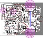
I like your layout.
You could leave more space between the 2n3019 , to be able to mount a cooler. I my build the bd140 run quite hot too ...
Thanks. You could see that there are lots of modifications.
Leaving more space between 3019's was in my mind too, but I considered its side effects. An alternative version that may have ~10mm gap is possible due to request.
BD140's are hot indeed but stays still in modest levels.
Last edited:
Terra, your PCB has the same amount of gain 10k/470.
I meant open-loop gain.
Elvee's brief:
http://www.diyaudio.com/forums/solid-state/189599-my-little-cheap-circlophone-62.html#post2892681
Thanks. You could see that there are lots of modifications.
Leaving more space between 3019's was in my mind too, but I considered its side effects. An alternative version that may have ~10mm gap is possible due to request.
BD140's are hot indeed but stays still in modest levels.
Suitable big inexpensive schottky diodes include SR504, SB540. The 50v and 60v editions have a less optimal voltage drop pattern, according to the datasheets. We're not utilizing the reverse voltage tolerance anyway and so a 20v model could do fine. For derating at this area, higher amperage tolerance is primary consideration. If you play as loud as I do, SB360 is a bad idea twice because it is only 3a with extraneous voltage drop, and so that sort of derating is not as helpful as an SR502, which is 5a with much less voltage drop. See the datasheets for forward voltage versus current charts.
For reference, consider that Polarized power caps on this same circuit have reverse tolerance of about 1v or less so it is fortunate that we're not consuming reverse voltage tolerances in this area.
At the area of 3019, there is heat pooling that could be resolved with a fan or with more favorable spacing or with adding drillings underneath the devices to allow airflow to remove the heat pooling. The resistors in that area also suffer heat pooling and should have a bit wider spacing.
At the area of BD140, there is heat pooling that could be resolved by adding 3 or 4 drillings underneath the heat spreader. However, we shouldn't use a heat spreader instead of a heatsink--A straight up wall gives minimalistic opportunity to conduct heat into air, since a heat spreader without a heatsink is a fast road to nowhere, and that plus no possible air movement, is why your drivers are hot.
Instead of so much heat, the BD140 heatsink should be a good size L-channel (or "T" channel) with holes in and under the L-channel to promote air movement, up, through, and around the heatsink. Then the drivers will stay cooler and decrease the risk of cooking the nearby passive parts.
Also, it would be great to have optional drillings so that the power caps could be located in such a way as to allow the BD140 heatsink to be wider than the board, and it would be nice to decrease capacitor heat exposure.
Last edited:
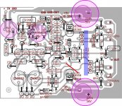
Ok, How about this?
16mm diameter decoupling capacitors still possible if output transistors should solder from bottom of pcb which is optimum case for this layout. PCB dimension is 75x55 mm. If it cut out as 75x58-60, decoupling caps can be supported more efficiently. In this case ground plate can be widened with a permanent marker.
16mm diameter decoupling capacitors still possible if output transistors should solder from bottom of pcb which is optimum case for this layout. PCB dimension is 75x55 mm. If it cut out as 75x58-60, decoupling caps can be supported more efficiently. In this case ground plate can be widened with a permanent marker.
Attachments
Last edited:
- Home
- Amplifiers
- Solid State
- ♫♪ My little cheap Circlophone© ♫♪