Hi,
I just read Ostripper's link about class B PCB mythodology. It looks like running the power rails close to eachother is not the full Eureka after all.
We might add that running power rails close to eachother includes a warning. Say each rail is about 75V, the potential gap between them is 150V. Running them just some mm apart from eachother is not safe as (in worst case) it could cause arcing.
It is true that in class B operation induction field cancellation (caused by the high currents) is not possible.
As this is about the induction field or current field
Is tension or voltage field of any importance? Is cancelling here of any importance? This is out of my knowledge but if anyone has the right answer it would be nice to know
cheers,
Olivier
High Olivier,
It is true that with the rail voltages involved caution must be used in running the rails together with PCB traces too closely spaced. These should be wide traces anyway, and one does not normally run wide traces extremely close to begin with. A 50-mil gap is fine.
I have apparently confused many people by using the term cancelation in referring to the nonlinear currents (and their magnetic fields) in the positive and negative supply rails of a class AB amplifier. Lets forget the term cancellation and just focus on the time-domain addition of the magnetic fields created by the close proximity of the positive and negative rails, as in the case where the wires are twisted together.
I'm sure you'll agree that the sum of the currents in the positive and negative rail leads is a decent approximation to a linear replica of the output signal current, in spite of the fact that each line carries a half-wave-rectified version of the signal. If the summed current is linear, the summed magnetic field will be linear, and thus ideally no distortion will be induced in other lines.
Cheers,
Bob
Hi bob,
The wires s current induced magnetic field will cancel only
if each wire carries the same current but in opposite direction.
Thus, in a class AB amp, there will be no cancellation if the wires
are twisted , unless this is a bridged amp where one amp s
rail is twisted with the other amp s opposite rail...
As for class AB, one wire s magnetic field will simply
be induced in the other wire totaly in phase,
reducing in some extent the rail to rail AC variation
since the same AC signal will be applied to the rails;
though the AC signal in respect to ground will
stay exactly the same.
cheers,
Hi wahab,
Once again, I have lent confusion by referring to cancellation of the nonlinear frequency components of the magnetic fields of the two rail wires when twisted together. I never meant to imply that the fundamental signal was somehow canceled. It is best just to visualize this action in the time domain. The two magnetic fields SUM to a linear representation of the signal, and that summed magnetic field is less likely to induce nonlinear signal energy into other circuits.
Cheers,
Bob
Hi Bob,
Problem is that in a class AB amp, time domain wise,
only ONE rail produce a magnetic field at a given moment
while at the same moment the other rail produce no magnetic
field since there s no current flowing through it...
Thus, the non active rail will simply act as a secondary coil ,
transforming the magnetic field it receive to a voltage/current
that will add to the normal rail voltage.
This amount as injecting the same perturbation in the inactive
rail, the perturbation phase being of course the same in the
two conductors, but not the amplitude.
cheers,
High Olivier,
................
I have apparently confused many people by using the term cancelation in referring to the nonlinear currents (and their magnetic fields) in the positive and negative supply rails of a class AB amplifier.
...............
Cheers,
Bob
Hi Bob,
Don't worry, you didn't confuse me at all. It's crystal clear that only harmonics are canceled, while the magnetic field of the fundamental is still there.
Hi Bob,
.................
Thus, the non active rail will simply act as a secondary coil ,
transforming the magnetic field it receive to a voltage/current
that will add to the normal rail voltage.
.................
cheers
Hi Wahab,
It's true that the magnetic field from the active supply rail will do something with the inactive supply rail. But as the latter is an open circuit (it's inactive), it only will induce a voltage (thus no current), which has no further effect.
Cheers,
E.
I did not mean to "stir the pot" with the link. The basic theory of what happens with a twisted rail pair was always quite oblivious. Perhaps , GK's statement "it will never be perfect" and the fact that any circuitry affected by said fields has no business being near them anyway reflect on the point. The "point" being ... with the proper layout (high current section physically separated - even on the same board) , would this be a significant distortion factor ?
Who would run a high impedance trace near a high current one ? Where I see no twisted wires (OEM's), they run cabling between steel chassis layers. Usually , the power supply/OP stage and any low level circuitry are on separate boards and sometimes even separated by steel chassis members. Aluminum cases might not be as effective. In OEM aluminum cases , I've seen strategically placed steel dividers and "cages" (trafo's /AC-line components) to deal with this shortcoming.
OS
Run the OP signal on the shield, as well ... effective. I just run a stupid "purple wire" across my low imp. output board (below - blue line) , no issues.
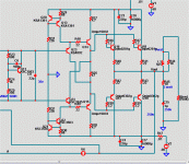
Bob , my question is about your DBT triple (ch. 10 /page 192-3 - figure 10.6 and 10.7). You show the current sources , but what "flavor" (led , 2Q , diode). In other words , what would be the best temperature coefficient CCS to match with this excellent OP stage ? No basestoppers ? , I'll leave pads for them... I know better. Also , you run the drivers at 50ma ... is this to set a stable operating temperature for the vbe cancellation of pre/driver ?
As you see below , I will build it ... I have the all the pre/drivers separately coupled to a small PCB aluminum bar (to-126 opposes the to-220). With this much Beta , I will be able to try the hawksford cascode properly (luxman).
PS - I will initially use it as a sub amp (it might have some fidelity as well - next amp
OS
Hi OS, I apologize for failing to respond to this post. I have not given a lot of thought to what is the best current source for I1 and I2 for the folded emitter followers in the Diamond Buffer Triple output stage. I don't think they are very critical. A feedback current source, where one Vbe is impressed across the emitter resistor seems to work well, since it has a fairly high output impedance and does a decent job of preserving voltage headroom. Its current will decrease as temperature increases. The current through drivers Q3 and Q4 will also tend to decrease with temperature since R1 has approximately 2 Vbe across it, so I guess this is a good thing.
I run the drivers at 60 mA because I like to run drivers hot so that there will be plenty of current to turn off the output transistors under conditions of high output current slew rate.
There are no base stoppers in these figures for simplicity of the drawing.
Cheers,
Bob
No problem , Bob. If I was in the "warm water", I would not respond... either
. I simulated the triple with a pair of 2Q CCS's and ksa992/sc1845's (lower Vceo - real low Cob). I would prefer a to-126 package to thermally couple to the MJE's (any suggestions ? ).
My circuit (below 1).
My first attempt (below 2) OOOps ! standard oscillator.
With R48-49 stoppers on the drivers (below 3) , things started to come alive
With njw0281/0302's just about as economical as the MJE's ($2.30 vs 1.90) , I'll might use them as the drivers ! No problem driving those 4-8 pair of outputs then , unlike some on the forum who try that with just EF2's (droop)
.OS
Attachments
Hi Bob,
Problem is that in a class AB amp, time domain wise,
only ONE rail produce a magnetic field at a given moment
while at the same moment the other rail produce no magnetic
field since there s no current flowing through it...
Thus, the non active rail will simply act as a secondary coil ,
transforming the magnetic field it receive to a voltage/current
that will add to the normal rail voltage.
This amount as injecting the same perturbation in the inactive
rail, the perturbation phase being of course the same in the
two conductors, but not the amplitude.
cheers,
Hi wahab,
We still seem to have trouble communicating on this, in spite of the fact that we are both reasonably smart people. I'm befuddled. I think that what is confusing you and Glen is your focus on the fact that half the time the non-active rail is not carrying current. Focus instead on the fact that the SUM of the currents in the plus and minus rails adds to a linear representation of the signal that will not create a lot of distortion if its magnetic field is induced into something nearby.
If the two rails (or the two groups of output transistors) are not grouped closely, a victim conductor will have induced in it voltages by each of the magnetic fields from the positive and negative circuits. However, those magnetic field strengths will likely not be equal because net distance from the separated positive and negative magnetic aggressors will be different. So at the victim those fields will not sum to a linear representation. In the extreme, one would get all of the magnetic field from the positive portion of the output stage and none of the magnetic field from the negative side of the output stage. One such magnetic field by itself, being half-wave in its origin, will be extremely nonlinear.
The distortion mechanism from nonlinear magnetic fields in the output stage of a class AB amplifier is especially insidious. It requires good layout to minimize it, and keeping the positive and negative generating halves of the mechanism in close proximity to one another is only one layout precaution that needs to be taken to minimize the effect of this insidiuos distortion. There will still be examples where people successfully get this source of distortion down by good layout practices without the steps I have discussed here, but that is no reason not to consider using those steps as a major weapon against this distortion.
I urge you to read Cherry's excellent paper on this subject. This is certainly not mythology.
Cheers,
Bob
post1787.
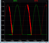
the graphs have confused me.
I can't find R26 (pre-driver current varying from 27.2uA to 28.6uA i.e. +-0.7uA)
R35 does not measure Driver current. Ir35 shows up the variation in the bias voltage as the feedback tries to correct for the different drive requirements of the ClassAB output stage to maintain low distortion during the crossover.
You need to add in a dummy resistor on the Emitters of the drivers to read Driver current.
Why are the peak R35 currents varying alternately when the output is changing from +ve flow to -ve flow cf. from -ve flow to +ve flow?
but this considers only the "FLOW" half of the "CIRCUIT".Focus instead on the fact that the SUM of the currents in the plus and minus rails adds to a linear representation of the signal that will not create a lot of distortion if its magnetic field is induced into something nearby.
The "RETURN" half is just as important. This is either the Power Ground current or the Speaker RETURN current.
To minimise the effects of radiated fields the flow and return pair must be of small radiating area. I refer to this as the twisted triplet, (+ve, -ve, return).
It's just the same at the receiving end.
The FLOW & RETURN of the signal pair must be of small receiving area.
Hi wahab,
.....................
There will still be examples where people successfully get this source of distortion down by good layout practices without the steps I have discussed here,
Hi Bob,
That right. Instead of cancellation of the harmonics at the source of all evil, one can make the receiving part (i.e. the input stage) insensitive to magnetic induction by using a proper PCB layout. Cherry described this too.
but that is no reason not to consider using those steps as a major weapon against this distortion.
................
Cheers,
Bob
Sure. I would say just apply both techniques (to be on the safe side).
Cheers,
E.
Last edited:
In Addtion to AndrewT and Edmond_Stuart, emitting loop area and receiving loop area are both important in this regard.
I was surprized after Cherry´s article that quite often as solution for this problem the power supply rail twist was offered, because it does normally not include all of the current for the cancellation action.
Straight forward analysis should reveal which elements and wires (pcb traces) do form the emitting loop and this includes the output summing trace and the speaker wiring.
Sometimes the solution seems counterintuitive and may be impractical to some extent, so Edmond´s advice to minimize the receiver loop area too and to avoid impedance coupling effects in this loop is surely a good one.
Hi Bob,
That right. Instead of cancellation of the harmonics at the source of all evil, one can make the receiving part (i.e. the input stage) insensitive to magnetic induction by using a proper PCB layout. Cherry described this too.
Sure. I would say just apply both techniques (to be on the safe side).
Cheers,
E.
Hi Edmond,
Thanks for pointing this out. That is good advice. Magnetic induction is a really insidious source of distortion that can make an otherwise-great design suffer needless impairment to performance.
Cheers,
Bob
insidious distortion
Hi Bob,
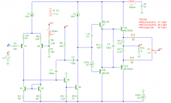
Not sure whether you are aware of a third method to reduce this insidious distortion: by means of my 'magic little pot'. So I mention it again (I hope not ad nauseum). See the pic below, red encircled stuff.
Without induction from the power rails this simple 'blameless' amp shows a THD20 of 41.7 ppm.
Next, I have simulated this insidious mechanism by inserting two inductors (100nH) into the pos. rail and the global FB path, which are loosely coupled (K=0.1). Now THD20 rises to 95.2 ppm.
And finally, I have added the magic pot (10 Ohms, wiper at 75%*), which brought back the THD level to its original value (and even slightly below): 36.7 ppm.
Cheers,
E.
* 75% is also optimal at 10kHz. So it is not frequency dependent.
Hi Edmond,
Thanks for pointing this out. That is good advice. Magnetic induction is a really insidious source of distortion that can make an otherwise-great design suffer needless impairment to performance.
Cheers,
Bob
Hi Bob,
Not sure whether you are aware of a third method to reduce this insidious distortion: by means of my 'magic little pot'. So I mention it again (I hope not ad nauseum). See the pic below, red encircled stuff.
Without induction from the power rails this simple 'blameless' amp shows a THD20 of 41.7 ppm.
Next, I have simulated this insidious mechanism by inserting two inductors (100nH) into the pos. rail and the global FB path, which are loosely coupled (K=0.1). Now THD20 rises to 95.2 ppm.
And finally, I have added the magic pot (10 Ohms, wiper at 75%*), which brought back the THD level to its original value (and even slightly below): 36.7 ppm.
Cheers,
E.
* 75% is also optimal at 10kHz. So it is not frequency dependent.
Attachments
Hi wahab,
We still seem to have trouble communicating on this, in spite of the fact that we are both reasonably smart people. I'm befuddled. I think that what is confusing you and Glen is your focus on the fact that half the time the non-active rail is not carrying current. Focus instead on the fact that the SUM of the currents in the plus and minus rails adds to a linear representation of the signal that will not create a lot of distortion if its magnetic field is induced into something nearby.
If the two rails (or the two groups of output transistors) are not grouped closely, a victim conductor will have induced in it voltages by each of the magnetic fields from the positive and negative circuits. However, those magnetic field strengths will likely not be equal because net distance from the separated positive and negative magnetic aggressors will be different. So at the victim those fields will not sum to a linear representation. In the extreme, one would get all of the magnetic field from the positive portion of the output stage and none of the magnetic field from the negative side of the output stage. One such magnetic field by itself, being half-wave in its origin, will be extremely nonlinear.
The distortion mechanism from nonlinear magnetic fields in the output stage of a class AB amplifier is especially insidious. It requires good layout to minimize it, and keeping the positive and negative generating halves of the mechanism in close proximity to one another is only one layout precaution that needs to be taken to minimize the effect of this insidiuos distortion. There will still be examples where people successfully get this source of distortion down by good layout practices without the steps I have discussed here, but that is no reason not to consider using those steps as a major weapon against this distortion.
I urge you to read Cherry's excellent paper on this subject. This is certainly not mythology.
Cheers,
Bob
Hi Bob,
Thanks for this extended explanation.
The principle look valid , although as you pointed it, preventing
magnetic fields from radiating on sensitive parts of the design
is surely the most efficient solution..
As an eventual solution, putting big caps near the OS with a low R
resistor in serial with the supply rail..
This will not prevent magnetic fields but the wire path current
waveform will be better integrated (mathematically speaking)
and thus, the AC current variation due to signal currents will
be of lower amplitude and longer period through the said wire,
allowing to be closest to a statical magnetic field caracteristics..
Hi Wahab,
It's true that the magnetic field from the active supply rail will do something with the inactive supply rail. But as the latter is an open circuit (it's inactive), it only will induce a voltage (thus no current), which has no further effect.
Cheers,
E.
Hi Edmond,
The inactive rail wire is not an open circuit, it s in serial with the power supply output and the load,i.e, the amp.
As such, any current or voltage (this is the same) variation will be added/substracted to the supply voltage/current of the power PS
inactive rail , seen from the amp.
cheers,
w
Hi Wahab,
The load comprises two parts:
1. The collectors of the OPS, a high impedance when turned off. So any induced voltage will not result in a significant amount of current.
2. the front-end.
2a. If it's powered by a separate PSU it has (obviously) no effect.
2b. If it is powered by the main PSU via serial regulators, the input represent also a high impedance. Ergo little or no effect.
2c. If it is powered via an RC filter network from the main PSU also little or no effect (because the induced voltage is filtered away).
2d. If it is powered directly from the main PSU, you might have a big problem. For example with the amp as posted on p. 1794. In this case the VAS compensation is referenced to the negative supply rail. So any voltage on this rail has an (devastating) effect on the performance.
Bottom line: it all depends on the circuit details.
Cheers,
E.
Hi Bob,
Not sure whether you are aware of a third method to reduce this insidious distortion: by means of my 'magic little pot'. So I mention it again (I hope not ad nauseum). See the pic below, red encircled stuff.
Without induction from the power rails this simple 'blameless' amp shows a THD20 of 41.7 ppm.
Next, I have simulated this insidious mechanism by inserting two inductors (100nH) into the pos. rail and the global FB path, which are loosely coupled (K=0.1). Now THD20 rises to 95.2 ppm.
And finally, I have added the magic pot (10 Ohms, wiper at 75%*), which brought back the THD level to its original value (and even slightly below): 36.7 ppm.
Cheers,
E.
* 75% is also optimal at 10kHz. So it is not frequency dependent.
Hi Edmond,
This is very nice solution, but with of little use for DIY. Not so many DIYers have distortion analyzer, and specially for so low distortion levels.
How to adjust that trimer pot with no distortion analyzer??
dado
Hi Dado,
Good point. I also don't have an AP. But with a good sound card you can measure THD levels at about 10 ppm. With the best sound card you can get (Lynx L22) and specialized software and additional filters you can measure as low as 0.1ppm, though not that easy and time consuming.
Cheers,
E.
Good point. I also don't have an AP. But with a good sound card you can measure THD levels at about 10 ppm. With the best sound card you can get (Lynx L22) and specialized software and additional filters you can measure as low as 0.1ppm, though not that easy and time consuming.
Cheers,
E.
Hi Dado,
Good point. I also don't have an AP. But with a good sound card you can measure THD levels at about 10 ppm. With the best sound card you can get (Lynx L22) and specialized software and additional filters you can measure as low as 0.1ppm, though not that easy and time consuming.
Cheers,
E.
Hello Edmond
This 0.1ppm is it at 20Khz.
Regards
Arthur
- Home
- Amplifiers
- Solid State
- Bob Cordell's Power amplifier book