Except that the FB around the OPS is the same in both cases, I do NOT agree with your assertions.
So since you agree that the feedback is the same in both cases, what is it precisely that you disagree with?

You can find the answer here:How is the comparison invalid?
http://www.diyaudio.com/forums/soli...lls-power-amplifier-book-128.html#post2418623
calculating the lead compensation
Hi Joakim,
Using your formulas to calculate the lead compensation for the TPC compensation seems okay for C1 < C2. However, for C1 > C2, the step response is way too slow, IOW, I did something wrong.
Here's my calculation:
C1 = 600pF (input cap)
C2 = 120pF (output cap)
R1 = 530R
Rfb1 = 3k8
Rfb2 = 200R
Rp = Rfb1 || Rfb2 = 190R
A = 20
RE = 68R
Ic = 2.5mA
gm = 1/(68+10) = 12.8mA/V
tau0 = A * C1 / gm = 20 * 600 / 12.8 = 937 ns
tau1 = R1 * ( C1 + C2 ) = 382 ns
tua2 = tau0 + tau1 = 1319 ns
lead compensation, R3 and C3:
R3 = tau2 * Rp - tau1 * Rfb1 / (-tau0) = ( 1319*190 - 382*3800 ) / (-937) = 1282R
C3 = tau2 / ( R3 + Rfb1 ) = 1319 / ( 1282 + 3800 ) = 260 pF
Clearly, these values are wrong, but why?
(BTW, pen and paper math is not my forte. Actually, I hate it, as it's so prone to errors)
So please, would you be so kind to pinpoint my error?
Cheers,
E.
I do not understand your arguments.
TMC as TPC are minor loop compensation techniques
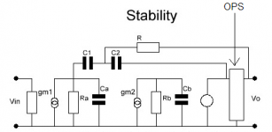
Did you look at figure (2) of my hand written notes where the TMC circuit is drawn in a nonstandard way? That might help understand why I did not treat it as a nested feedback loop circuit.
If you still want to use a minor/major loop analysis method then it's that you didn't account for the output stage that I object too. The stability of the major loop is well predicted by your previous analysis as long as the local feedback from the OPS to the VAS through R is stable with good margin and the OPS pole is well above the major loop crossover frequency. There is a need to check that the minor loop enclosing the OPS and VAS is stable too and has good enough margin.
Attachments
There are no answers there. Just incoherent rumblings.
Hi Mike,
Earlier I suggested that you post some up-to-date, ready-to-run amplifier simulations to illustrate the veracity of your points. If you would do that, I think that people would attach more credibility to what you are saying. Replying to a post with little more than a link to some previous post, often in another thread, and often from long ago, and often with no interpretive results, is not helpful. If you are the one who wants to make a point, it is up to you to do the work to make it clear and credible.
Arguing about how much loop gain surrounds the output stage does not make your point - there is more to it. I believe that only a full simulation can really cut through the hand-waiving. Even then, great care is needed in interpreting the comparative stability results. Also, as pointed out earlier, CCIF IM results should also be considered, as they do not always track THD results (partly due to the fact that the feedback factor is usually larger at the IM frequencies, which are lower than the harmonic frequencies.
Cheers,
Bob
Hi Joakim,
Using your formulas to calculate the lead compensation for the TPC compensation seems okay for C1 < C2. However, for C1 > C2, the step response is way too slow, IOW, I did something wrong.
Hi!
Those are not the C1, C2 and R values in a TPC circuit but the values you would have used in a TMC circuit. This calculation then gives you the lead compensation required in a TPC amplifier with the same C1, C2 and R to give it the same response.
After you have done that it is possible to change C1', C2' and R' in the TPC network to another combination which keeps the VAS transimpedance
Z(s) = - D (s tau3 + 1) / (s^2), where tau3 = R' (C1'+C2') = tau1 and D = 1 / (R' C1' C2'),
the same. For example, you can switch C1' and C2' around or make both the same value (in that case R changes too) to decrease the loading of the VAS.
The way I'd design the comonent values of the TPC circuit is instead to start by selecting a crossover frequency and then choose tau2 to give me a good enough phase margin. The phase margin becomes atan (tau2 wc) minus the excess phase shift of the OPS, VAS and LTP at the crossover frequency where wc = 2 * pi * loop crossover frequency. This follows from the loop gain expression
G_loop(s) = G(s) D (gm / A) (s tau2 + 1) / (s^2)
where
* G(s) is the output stage and load transfer function
* D = 1 / (R' C1' C2')
* gm is the LTP transconductance
* A is the feedback divider ratio
tau1 needs to be selected sufficiently shorter than tau2 for there to be no overshoot.
...incoherent rumblings.
Google says:
Did you mean: incoherent ramblings
. A higher IMD could be explained by a higher output current of the IPS (tanh distortion). This assumption is supported by the fact that if I increase the tail current (and also increase the emitter resistors to maintain the same gm), I get a lower IMD figure.
If I use a 5:1 capacitor ratio for the TPC case (and equal tail currents), then I get roughly the same IMD.
>but oddly, the mentioned frequencies, i.e, 1KHZ and 18/21KHZ didn't see their level reduced,
Hmm.... I did not observe this oddity. Due to different circuits and/or methods?
Cheers,
E.
hi, Edmond
Here the schematic i used along with the TMC IMD sims.
As displayed, reducing the IPS degeneration, that is increasing
gm by a factor of 2 clearly show that all intermodulation products
are reduced whatever the frequency, safe the mentionned ones,
ie, 18/21KHZ and the 1KHZ products.
This show that IPS loading is not the culprit.
Reducing the input vas cap from 47 to 22pF reduce dramatically
the discussed products, leading to think that IMD was generated
by an insufficent slew rate in the VAS or VAS+OPS, as i still didn t
check the exact source of this distorsion...
On the other hand, a TMC network using some marginal TPC
allow for the lowest level of THD and very low IMD , but this latter
type of distorsion seems a little better on the TPC only variant.
Useless to say that CMC has catastrophic IMD scores, as already
displayed in the previous IMD sims i posted.
cheers,
w
Attachments
Hi!
Those are not the C1, C2 and R values in a TPC circuit but the values you would have used in a TMC circuit.
Hi Joakim,
Okay, not the same values as in a TPC circuit.
This calculation then gives you the lead compensation required in a TPC amplifier with the same C1, C2 and R to give it the same response.
[snip]
Now, I'm really puzzled. First, they are not the same and now they are the same?
Cheers,
E.
Hi Bob, you are right, but from where I sit I have seen little to nothing of an unbiased or clear analysis/results from both sides in this (otherwise interesting) debate. It appears to me that, rather than finding the truth, proving by any means (including sometimes deception!) the other side wrong is the ultimate goal in this endless debate.Earlier I suggested that you post some up-to-date, ready-to-run amplifier simulations to illustrate the veracity of your points. If you would do that, I think that people would attach more credibility to what you are saying. Replying to a post with little more than a link to some previous post, often in another thread, and often from long ago, and often with no interpretive results, is not helpful. If you are the one who wants to make a point, it is up to you to do the work to make it clear and credible.
E.g. you posted simulations based on an (eventually admitted) arbitrary suboptimal TPC implementation, without (at that time) the details (like models) that would allow one to reproduce your results.
Then Edmond, in another thread, after ranting and calling other people names for alleged errors (and also presenting deceptive and usupported numbers),
ends up admitting that TMC extra loads the IPS (and therefore more current and degeneration is required to compensate).Edmond Stuart said:>On the flip side, TMC extra loads the input stage, with the equivalent lead-lag compensation network Miller reflection. For identical global amp> results, this may require a beefier input stage (more current, more degeneration, etc...) compared to simple Miller or TPC compensation.
Is that So? Let's have a look at the (simmed) output current of the input stage for a typical blameless amp with respectively Miller, TPC and TMC compensation. f=100kHz and Vi=1VMiller: 261.0nATPC: 265.9nATMC: 260.5nASo TMC results in the lowest IPS output current of all of the three compensation schemes. Needless to say that I've no trouble with this alleged 'flip side'.
Edmond Stuart said:The funny thing is that regarding TMC, THD is slightly lower and IMD is slightly higher compared to TPC. A higher IMD could be explained by a higher output current of the IPS (tanh distortion). This assumption is supported by the fact that if I increase the tail current (and also increase the emitter resistors to maintain the same gm), I get a lower IMD figure.If I use a 5:1 capacitor ratio for the TPC case (and equal tail currents), then I get roughly the same IMD.
I think there's little chance in getting anything very useful from this debating style. It would be interesting if anybody from the TPC team could build a bulleted list of TMC pros and cons against TPC and the metric/reasoning beyond. Things like "concerned about", "makes me feel nervous" do not count. Such a list could be the basis for further debate and mods. Is this to much to ask for?
Last edited:
Hi Mike,
Earlier I suggested that you post some up-to-date, ready-to-run amplifier simulations to illustrate the veracity of your points. If you would do that, I think that people would attach more credibility to what you are saying. Replying to a post with little more than a link to some previous post, often in another thread, and often from long ago, and often with no interpretive results, is not helpful. If you are the one who wants to make a point, it is up to you to do the work to make it clear and credible.
Arguing about how much loop gain surrounds the output stage does not make your point - there is more to it. I believe that only a full simulation can really cut through the hand-waiving. Even then, great care is needed in interpreting the comparative stability results. Also, as pointed out earlier, CCIF IM results should also be considered, as they do not always track THD results (partly due to the fact that the feedback factor is usually larger at the IM frequencies, which are lower than the harmonic frequencies.
Cheers,
Bob
Hi Bob,
Well said. However, did you notice that he has used equal caps in the TMC compensation? This explains why he erroneously thinks that TMC is inferior to TPC. With such a bad choice of caps, of course TMC can't be competitive.
Cheers,
E.
Okay, not the same values as in a TPC circuit.
What I mean is that my calculation is not a calculation of the optimal lead compensation for a TPC circuit with certain C1, C2 and R but the lead compensation needed for the TPC circuit to give it the same response as a TMC circuit with equal values of C1, C2 and R.
If you choose like you did in your post
C1 = 600pF (input cap)
C2 = 120pF (output cap)
R = 530R
then you are making a TPC circuit with the same response as a TMC circuit with those values. And that's probably not what you wanted.
hi, Edmond
Here the schematic i used along with the TMC IMD sims.
As displayed, reducing the IPS degeneration, that is increasing gm by a factor of 2 clearly show that all intermodulation products are reduced whatever the frequency, safe the mentioned ones, ie, 18/21KHZ and the 1KHZ products. This show that IPS loading is not the culprit.
[snip]
cheers,
w
Hi wahab,
I'm afraid you are jumping too fast to conclusions. Increasing gm by a factor of 2 will indeed reduce IMD, of course. But decreasing RE will also increase the IPS non-linearity. Now, the question is which of the two mechanisms has the most impact?
I've repeated your experiments with RE is 33R respectively 100R, though the rest of my circuit is slightly different.
with RE=100R I got the following IMD products:
1kHz: 228 ppb
18kHz: 757 ppb
21kHz: 846 ppb
and with RE=33R:
1kHz: 330 ppb
18kHz: 567 ppb
21kHz: 615 ppb
As you see, these figures are a bit ambiguous. The increase at 1kHz (with RE=33) could be explained by an increased non-linearity of the IPS, which overrules the beneficial effects of a higher gm. Ergo, the non-linearity of the IPS is at stake. IOW, the IPS loading does have a not insignificant effect.
Cheers,
E.
Did you look at figure (2) of my hand written notes where the TMC circuit is drawn in a nonstandard way? That might help understand why I did not treat it as a nested feedback loop circuit.
If you still want to use a minor/major loop analysis method then it's that you didn't account for the output stage that I object too. The stability of the major loop is well predicted by your previous analysis as long as the local feedback from the OPS to the VAS through R is stable with good margin and the OPS pole is well above the major loop crossover frequency. There is a need to check that the minor loop enclosing the OPS and VAS is stable too and has good enough margin.
Of course the minor loop must be stable. If you look at the loop gain of the minor loop, at frequencies close to crosse over, the R is shorted to the input of the output stage by the large C2 and do not influence the minor loop stability anymore. The minor loop loop gain is governed by C1 only like in a Miller minor loop.
Is this wrong ?
JPV
That's true for the minor loop enclosing just the VAS. At its crossover frequency which can be pretty high, maybe tens of MHz, R is basically shorted out and you have only C1 and C2 in series.
But there is also the loop around the output stage that has to be stable. This loop can become unstable as you decrease R even though the VAS looks stable at its local loop crossover frequency where 1/(s C2) << R.
But there is also the loop around the output stage that has to be stable. This loop can become unstable as you decrease R even though the VAS looks stable at its local loop crossover frequency where 1/(s C2) << R.
Last edited:
That's true for the minor loop enclosing just the VAS. At its crossover frequency which can be pretty high, maybe tens of MHz, R is basically shorted out and you have only C1 and C2 in series.
But there is also the loop around the output stage that has to be stable. This loop can become unstable as you decrease R even though the VAS looks stable at its local loop crossover frequency where 1/(s C2) << R.
But the loop gain around the output stage is less than 1 so no instability.
JPV
The loop gain around the output stage is, with the "global loop" back through the IPS broken
times the gain of the output stage itself, so that is not correct. If all other feedback paths are in place it looks like in andy_c:s post and has a double-pole, single zero type response. See also the equation in my previous reply.
Code:
     (  + C1)
-------------------
 (  + C2 C1 R1 ) s
times the gain of the output stage itself, so that is not correct. If all other feedback paths are in place it looks like in andy_c:s post and has a double-pole, single zero type response. See also the equation in my previous reply.
What I mean is that my calculation is not a calculation of the optimal lead compensation for a TPC circuit with certain C1, C2 and R but the lead compensation needed for the TPC circuit to give it the same response as a TMC circuit with equal values of C1, C2 and R.
If you choose like you did in your post
C1 = 600pF (input cap)
C2 = 120pF (output cap)
R = 530R
then you are making a TPC circuit with the same response as a TMC circuit with those values. And that's probably not what you wanted.
Ah, now I got it, thanks!
Cheers,
E.
- Home
- Amplifiers
- Solid State
- Bob Cordell's Power amplifier book